
Cyberface - the first commercial HMD
Get Started for FREE
Sign up with Facebook Sign up with X
I don't have a Facebook or a X account


|
Scooped by
Sara Mautino
onto HMD hot spot June 28, 2016 10:03 AM
|

 Your new post is loading...
 Your new post is loading...
Your new post is loading...

The Myo armband senses muscle and arm movements to control apps using gestures. We took it apart to check out the hardware and unique construction.
From
www

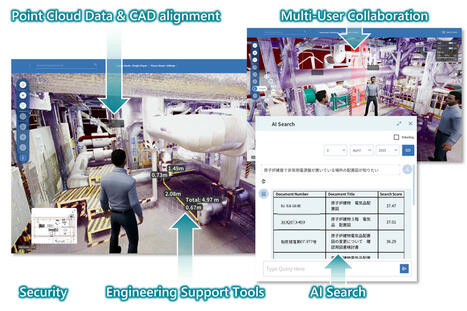
Hitachi’s Metaverse Platform for Nuclear Power Plants enhances collaboration among stakeholders, streamlines design and construction workflows, and supports the development of practical and effective investment plans by integrating metaverse and AI technologies.
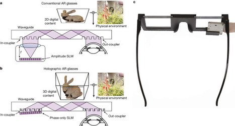
Full-colour 3D holographic augmented-reality displays with metasurface waveguides
Emerging spatial computing systems seamlessly superimpose digital information on the physical environment observed by a user, enabling transformative experiences across various domains, such as entertainment, education, communication and training1–3. However, the widespread adoption of augmented-reality (AR) displays has been limited due to the bulky projection optics of their light engines and their inability to accurately portray three-dimensional (3D) depth cues for virtual content, among other factors4,5. Here we introduce a holographic AR system that overcomes these challenges using a unique combination of inverse-designed full-colour metasurface gratings, a compact dispersion-compensating waveguide geometry and artificial-intelligence-driven holography algorithms. These elements are co-designed to eliminate the need for bulky collimation optics between the spatial light modulator and the waveguide and to present vibrant, full-colour, 3D AR content in a compact device form factor. To deliver unprecedented visual quality with our prototype, we develop an innovative image formation model that combines a physically accurate waveguide model with learned components that are automatically calibrated using camera feedback. Our unique co-design of a nanophotonic metasurface waveguide and artificial-intelligence-driven holographic algorithms represents a significant advancement in creating visually compelling 3D AR experiences in a compact wearable device. We develop a method for providing high-quality, holographic, three-dimensional augmented-reality images in a small form factor suitable for incorporation in eyeglass-scale wearables, using high-refraction-index glass waveguides with nanoscale metasurfaces, and incorporating artificial intelligence.
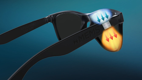
xMEMS Labs has expanded its µCooling fan-on-a-chip platform into XR smart glasses.

From
www
US 20250199317 A1 - Head-Mounted Display With Volume Substrate-Guided Holographic Continuous Lens Optics Published 19.06.2025:
This application relates to a see-through head-mounted display using recorded substrate-guided holographic continuous lens (SGHCL) and a microdisplay with laser illumination. The high diffraction efficiency of the volume SGHCL creates very high luminance of the virtual image.

"Project Aria is a research program from Meta, to help build the future responsibly. Project Aria unlocks new possibilities of how we connect with and experience the world.

From
www
US20220215375 - Smart-glasses based contactless automated teller machine (“ATM”) transaction processing
A method for touchless communication between an ATM and a smartglasses device worn by a user is provided. The method may be executed at the smartglasses device. The method may include identifying a current global positioning system (“GPS”) location of the ATM. The method may include communicating with an external database to determine an ATM identifier associated with the ATM. The ATM identifier may include ATM communication data. The method may include transmitting an external smartglasses identifier to the ATM via the ATM communication data. The method may include receiving a communication from the ATM. The communication may include an interactive payment interface. The method may include displaying the interactive payment interface on the smartglasses. The method may include receiving one or more commands from the user. The method may include transmitting the one or more commands from the smartglasses to the ATM.

From
fortune
The form factor is nor truly lightweight nor "new" or "advanced", but, depending on the performances and possible affordances, the form factor may be a surprise Check https://www.spectacles.com , reminds a bit hashtag#Epson_Moverio tradition :-) see below* hashtag#smartglasses hashtag#hmd hashtag#arglasses hashtag#form_factor @Meta hashtag#Orion_glasses @Google hashtag#Android_XR_glasses @Apple *https://lnkd.in/dFVKCZsP
news press here:
Our award-winning lens inserts for XR provide sharp vision for both nearsighted and farsighted individuals with a simple slide, unlocking extended reality for individuals, families, and enterprises, eliminating the need to purchase multiple specialized—and wasteful—lenses. Embrace convenience and cost savings with an adjustable solution that can be shared by multiple users. This pioneering product is helping people experience the future together through adaptive VR/XR optimization. Currently compatible with Meta Quest 2, 3, and Lenovo VRX, additional models for Apple Vision Pro and HTC VIVE are in development.

Revolutionary new material for nano-imprint lithography promises to redefine augmented reality with enhanced performance and lower costs. Solnil has developed original inks enabling the preparation of dense high index (2 < n@520nm < 2.6) TiO2 material with very high transparency (loss < 0.1%). Selected as a recipient of the Horizon Europe EIC Transition Grant for the revolutionary METAPRINT project. METAPRINT was one of 40 projects chosen from over 400 submissions across 21 country participants. This initiative, titled "Nano-Imprint Lithography of Titania-Based Metaoptics," aims to redefine augmented reality (AR) by delivering next-generation smart-glass displays through unprecedented advances in nano-imprinting of nano-ceramics.

US20250020839 - EFFICIENT MODELING OF A DIFFRACTIVE WAVEGUIDE Abstract A method of simulating the optical performance of a diffractive waveguide includes, generating a plurality of transfer matrices for each diffractive grating of the plurality of diffractive gratings responsive to performing a diffraction modeling process for a plurality of diffractive gratings of the waveguide based on a plurality of input light rays each having at least a different first characteristic. A plurality of electric fields at outcoupling positions of an outcoupling grating of the plurality of diffractive gratings is determined based on the plurality of transfer matrices responsive to performing a ray tracing process for multiple instances of each input light ray of the plurality of light rays with at least a different second characteristic. A uniformity map is generated for the waveguide based on the plurality of electric fields. The uniformity map indicates a uniformity of one or more characteristics of the waveguide across different sampled pupil positions.

WO2025005768 - WEARABLE DISPLAY APPARATUS AND CONTROL METHOD THEREOF "Abstract (EN) A wearable display apparatus according to one embodiment of the present invention comprises: a communication unit which receives ultrasonic image data; a display unit which overlaps at least a portion of a lens unit and displays the ultrasonic image data as an ultrasonic image; and a control unit electrically connected to the lens unit, the communication unit, and the display unit, wherein the control unit can control at least one of the brightness or color of the display unit on the basis of image characteristics of the ultrasonic image data, and control the opacity of the lens unit on the basis of the position of a virtual region in which the ultrasonic image is displayed.

NUGGETS OF Augmented Reality #5 - DIFFRACTION GRATINGS Theory towards couple modes H. Kogelnik and C. V. Shank 1971 - Download as a PDF or view online for free

bharatdigital231@gmail.com's comment,
January 10, 12:49 AM
Transform your ideas into reality with our cutting-edge app development services. From concept to deployment, we specialize in creating feature-rich, user-friendly, and scalable mobile and web applications tailored to your unique needs. Whether it's a startup or an enterprise solution, we deliver seamless experiences across platforms with advanced technologies and intuitive designs. Let us help you bring your vision to life! https://bharatdigital.co/app-development/
|

From
observer
“We’ll continue investing in the people, talent and compute needed to make sure that we are set up for the opportunity ahead,” said CEO Sundar Pichai.
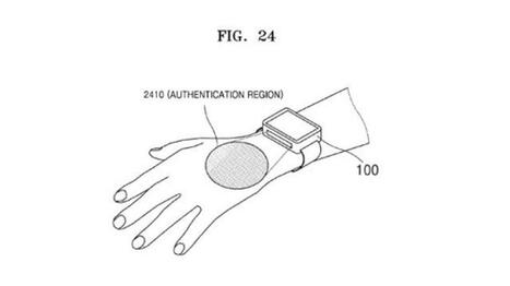
US20160034679 - Wearable device and method of operating the same - SAMSUNG ELECTRONICS CO., LTD.
Samsung has filed a patent for a wearable sensor that can read the user's veins to establish his or her identity. If implemented, this allows Samsung's future wearables to double as keys for doors and cars.

From
www
Shares of continuous glucose-monitoring device makers Abbott (ABT.N), opens new tab and Dexcom (DXCM.O), opens new tab were up 3.6% and 10%, respectively, in afternoon trading. Press conference with Centers for Medicare and Medicaid Services Administrator Mehmet Oz at the Department of Health and Human Services in Washington, D.C., U.S., June 23, 2025. REUTERS

Miniature Highland Cows Review's curator insight,
June 27, 9:01 PM
Are you searching for miniature Highland cows for sale? Look no further than Mary Highland Cattle Farm, your trusted source for premium, registered mini Highland cows that are as hardy as they are adorable. Whether you're looking to add a gentle, low-maintenance breed to your homestead or want a charming pasture companion, our miniature Scottish Highland cattle are the perfect choice. Why Choose Miniature Highland Cattle? Mini Highland cows (also called mini Scottish Highland cattle) are a smaller, friendlier version of the traditional Highland breed. With their signature long horns, thick double coat, and docile temperament, these cows are ideal for hobby farms, small acreage homesteads, and even as pasture pets. Benefits of miniature Highland cows: Hardy in all climates (especially cold, wet environments) Easy to handle and great with families Low maintenance and grass-fed Lifespan of up to 20 years Naturally disease-resistant These traits make them highly desirable among homesteaders, sustainable farmers, and animal lovers alike. Mary Highland Cattle Farm – Where Quality Meets Care At Mary Highland Cattle Farm, we specialize in mini Highland cows for sale that are: Genetically tested and vet-checked Raised on pasture and handled regularly for temperament Registered with recognized miniature cattle associations Available in a range of colors: red, dun, black, silver, and white Our farm is located in [Insert State/City for Local SEO], and we offer nationwide delivery options to bring your mini Highland calf or cow safely to your property. Browse Our Available Mini Highland Calves We currently have a selection of miniature Highland calves for sale, including: Heifer calves (female) Bull calves (male) Bred cows and cow-calf pairs Each calf is halter-trained, vaccinated, and accustomed to human interaction, making the transition to your farm smooth and stress-free. How to Reserve a Mini Highland Cow Reserving your mini Highland cow for sale is simple: Browse our available cattle online or schedule a farm visit. Contact us to ask questions or place a deposit. Arrange for local pickup or nationwide delivery. Our team is happy to guide you through the process and answer all your questions about raising Highland cattle. Frequently Searched Phrases We Answer: Mini Highland cows for sale near me Miniature Highland cattle for sale USA Buy Scottish mini Highland cow Small Highland cows for hobby farm Halter-trained mini Highland calves Mini Highland cows for sale with delivery If you've searched for any of the above, you're in the right place. Contact Mary Highland Cattle Farm Today Don’t miss your chance to own one of the most beloved heritage breeds in the world. Our mini Highland cows are waiting to become a part of your family or farm. � Email: info@maryhighlandcattle.com � Phone: +1 (912) 588-4644 � Websites: maryhighlandcattle.com maryhighlandcattlefarm.com Mary Highland Cattle Farm – Where tradition meets trust, and cuteness meets quality. https://maryhighlandcattle.com/product/available-mini-female-dwarf-goat-for-sale-at-mary-highland-cattle/ https://maryhighlandcattle.com/product/adorable-female-mini-donkey-for-sale/ https://maryhighlandcattle.com/product/female-miniature-highland-cow-for-sale/ https://maryhighlandcattle.com/product/male-mini-highland-cow-for-sale/ https://maryhighlandcattle.com/product/meet-bubbles-our-adorable-miniature-donkey-for-sale/ https://maryhighlandcattle.com/product/meet-candy-our-female-miniature-donkey-for-sale/ https://maryhighlandcattle.com/product/meet-champ-our-newborn-male-miniature-donkey-available-for-reservation/ https://maryhighlandcattle.com/product/mini-cattle-for-sale/ https://maryhighlandcattle.com/product/where-to-buy-mini-cows/ https://maryhighlandcattle.com/product/miniature-highland-cattle-for-sale/ https://maryhighlandcattle.com/product/micro-mini-highland-calf/ https://maryhighlandcattle.com/product/meet-fiona-our-newborn-miniature-donkey-book-now-for-reservation/ https://maryhighlandcattle.com/product/miniature-cattle-for-sale/ https://maryhighlandcattle.com/product/micro-mini-highland-cow/ https://maryhighlandcattle.com/product/mini-highland-cattle-for-sale/ https://maryhighlandcattle.com/product/miniature-donkey-for-sale/ https://maryhighlandcattle.com/product/mini-highlands-for-sale/ https://maryhighlandcattle.com/product/mini-highland-calf-for-sale/ https://maryhighlandcattle.com/product/female-mini-highland-cow-for-sale/ https://maryhighlandcattle.com/product/meet-lila-female-miniature-highland-cow-for-sale-book-now-for-reservations/ https://maryhighlandcattle.com/product/breeding-pair-of-miniature-donkeys-for-sale/ https://maryhighlandcattle.com/product/miniature-highland-cow-for-sale/ https://maryhighlandcattle.com/product/mini-highland-calf/ https://maryhighlandcattle.com/product/mini-highland-cows-for-sale/ https://maryhighlandcattle.com/product/our-male-mini-highland-cattle-for-sale/ https://maryhighlandcattle.com/product/meet-maisie-female-mini-highland-cow-for-sale/ https://maryhighlandcattle.com/product/mini-highland-heifer-calf/ https://maryhighlandcattle.com/product/highland-calf-for-sale/ https://maryhighlandcattle.com/product/meet-olive-our-adorable-female-mini-donkey-for-sale/ https://maryhighlandcattle.com/product/meet-oliver-our-newborn-male-mini-donkey-book-now-for-reservation/ https://maryhighlandcattle.com/product/scottish-highland-cattle-for-sale/ https://maryhighlandcattle.com/product/mini-dwarf-goat-for-sale/ https://maryhighlandcattle.com/product/meet-our-newborn-male-mini-dwarf-goat-book-now-for-reservation/ https://maryhighlandcattle.com/product/meet-paula-our-newborn-miniature-donkey-now-open-for-reservation/ https://maryhighlandcattle.com/product/mini-highland-calf-for/ https://maryhighlandcattle.com/product/miniature-highland-cows-for-sale/ https://maryhighlandcattle.com/product/scottish-highland-calf-for-sale/ https://maryhighlandcattle.com/product/mini-donkey-for-sale/ https://maryhighlandcattle.com/product/available-miniature-donkeys-for-sale/ https://maryhighlandcattle.com/product/meet-willow-female-mini-highland-cow-for-sale-book-now-for-reservations/ https://maryhighlandcattle.com/product/mini-cows-for-sale-near-me/ https://maryhighlandcattle.com/product/mini-dwarf-goat-now-available/

From
fortune
EssilorLuxottica has is the undisputed leader on everything to do with vision. How does a company commanding an entire industry continue to grow?

From
www
US20250181182 - Electronic Device Display With Array of Discrete Light-Emitting Diodes
An electronic device may include a display. The display may be formed by an array of light-emitting diodes mounted to the surface of a substrate. The substrate may be a silicon substrate. Circuitry may be located in spaces between the light-emitting diodes. Circuitry may also be located on the rear surface of the silicon substrate and may be coupled to the array of light-emitting diodes using through-silicon vias. The circuitry may include integrated circuits and other components that are attached to the substrate and may include transistors and other circuitry formed within the silicon substrate. Touch sensor electrodes, light sensors, and other components may be located in the spaces between the light-emitting diodes. The substrate may be formed from a transparent material that allows image light to reach a lens and image sensor mounted below the substrate.

From
www
US20250172815 - WAVEGUIDE COMBINER ASSEMBLIES FOR AUGMENTED REALITY OR VIRTUAL REALITY DISPLAYS SNAP inc. Pubblication of Application 29.05.2025 According to a first aspect of the invention, there is provided a waveguide combiner assembly for an augmented reality or virtual reality display, comprising: a waveguide combiner, having front and rear surfaces which are each substantially parallel to a waveguide plane, the direction normal to the waveguide plane being the waveguide axis, and the distance between the front and rear surfaces along the waveguide axis being the thickness of the waveguide combiner; a chassis including a support arm for supporting the waveguide combiner, the support arm defining a cavity between front and rear walls of the support arm which are spaced along a first direction by a distance greater than the thickness of the waveguide combiner, the waveguide axis and the first direction defining an offset angle between them which may be zero or non-zero, an edge portion of the waveguide combiner extending into the cavity; and at least one actively adjustable mounting structure configured to hold a respective point of the edge portion of the waveguide combiner at a selected position relative to the support arm, thereby enabling adjustment of the offset angle. In this way, the waveguide combiner integrated within the claimed waveguide combiner assembly can be spatially adjusted relative to the support arm of the chassis, thanks to the at least one actively adjustable mounting structure and without the external assistance of an external intricate optical jig and the use of glue to lock the waveguide combiner in position, which significantly eases the process of positioning the waveguide combiner and reduces the associated cost.

From
www
Optical arrangement for a display - US12222503B2 granted 02/2025

US20250028166 - APPARATUS FOR OPTICAL SEE-THROUGH HEAD MOUNTED DISPLAY WITH MUTUAL OCCLUSION AND OPAQUENESS CONTROL The invention consist of an optical see-through head mounted display (OST-HMD) device with opaqueness control and mutual occlusion capability
The present invention comprises a compact optical see-through head-mounted display capable of combining, a see-through image path with a virtual image path such that the opaqueness of the see-through image path can be modulated and the virtual image occludes parts of the see-through image and vice versa.

WO2025023933 - HYBRID REFLECTIVE AND DIFFRACTIVE WAVEGUIDE ARCHITECTURE To further minimize any image gaps at high frequencies, some embodiments of the hybrid waveguide system include a partially reflective thin film coating between the a high-refractive index substrate of a diffractive waveguide including the diffractive grating and a lower refractive index substrate of a reflective waveguide including the reflective grating structures.

US20250005620 - INDIVIDUAL-BASED MARKETING APPROACH IN THE METAVERSE ABSTRACT and CLAIMS "A method includes enabling a plurality of users to interact with a virtual world, each of the users represented as one or more avatars in the virtual world, obtaining preferences and consent of each of the users, displaying promotional messages to a user of the plurality of users in the virtual world based on the user's preferences and consent, and after displaying the promotional messages to the user, filtering the user's preferences and consent from the virtual world to remove transaction footprints."
20. The system of claim 19, wherein each of the users is represented as a virtual token in the virtual world.

US20250008656 - WIRE BONDING FOR MINIATURIZING PRINTED CIRCUIT INTERCONNECTION SUMMARY and CLAIMS Described herein are techniques for enabling wire bonding between different printed circuit modules. More specifically, printed circuit modules, including inflexible modules (e.g., having a printed circuit board (PCB) substrate) and/or flexible modules (e.g., having a flexible printed circuit (FPC) substrate) may be electrically connected using wire bonding. To do so, embodiments may utilize certain alignment techniques, reinforcement plates, and/or protective structures for the wire bonds, as described in the embodiments provided herein. Because wire bonding can have a pitch of less than 150 μm, the techniques herein can enable electronics to be miniaturized, which may enable devices (e.g., wearable devices) to have smaller form factors.
*** 1. An electronic device comprising: a first printed circuit module comprising: a first printed circuit substrate, and a first set of one or more bonding pads coupled to the first printed circuit substrate; a second printed circuit module comprising: a second printed circuit substrate, and a second set of one or more bonding pads coupled to the second printed circuit substrate; one or more wire bonds electrically connecting first set of one or more bonding pads to the second set of one or more bonding pads; and a protective structure covering at least a portion of the one or more wire bonds and coupled with the first printed circuit substrate and second printed circuit substrate. 2. The electronic device of claim 1, wherein the first set of one or more bonding pads are located on a first side of the first printed circuit substrate, and the second set of one or more bonding pads are located on a first side of the second printed circuit substrate, and wherein: a first portion of a reinforcement plate is coupled to a second side of the first printed circuit substrate opposite the first side of the first printed circuit substrate; and a second portion of the reinforcement plate is coupled to a second side of the second printed circuit substrate opposite the first side of the second printed circuit substrate. 3. The electronic device of claim 1, wherein the first printed circuit module is coupled to the second printed circuit module. 4. The electronic device of claim 3, wherein: the first set of one or more bonding pads are located on a first side of the first printed circuit substrate; the first printed circuit module comprises a cut-out extending from the first side of the first printed circuit substrate to a second side of the first printed circuit substrate opposite the first side of the first printed circuit substrate; and the one or more wire bonds extend through the cut-out from the first set of one or more bonding pads to the second set of one or more bonding pads. 5. The electronic device of claim 1, wherein the protective structure comprises a shielding can covering at least a portion of the one or more wire bonds. 6. The electronic device of claim 1, wherein the protective structure comprises a molding compound encapsulating the at least a portion of the one or more wire bonds. 7. The electronic device of claim 1, wherein the first printed circuit substrate, the second printed circuit substrate, or both, comprises a printed circuit board (PCB) substrate. 8. The electronic device of claim 1, wherein the first printed circuit substrate, the second printed circuit substrate, or both, comprises a flexible printed circuit (FPC) substrate. 9. The electronic device of claim 1, wherein the first set of one or more bonding pads, the second set of one or more bonding pads, or both, have a pitch of less than 100 microns. 10. A method of interconnecting printed circuits with wire bonding, the method comprising: forming one or more wire bonds electrically connecting one or more bonding pads of a first printed circuit module to one or more bonding pads of a second printed circuit module, wherein each of the first printed circuit module and the second printed circuit module comprise a respective printed circuit substrate; and forming a protective structure covering at least a portion of the one or more wire bonds, the protective structure coupled with the respective printed circuit substrate of each of the first printed circuit module and the second printed circuit module. 11. The method of claim 10, wherein the one or more bonding pads of the first printed circuit module are located on a first side of the respective printed circuit substrate of the first printed circuit module, and the one or more bonding pads of the second printed circuit module are located on a first side of the respective printed circuit substrate of the second printed circuit module, and wherein the method further comprises, prior to forming one or more wire bonds: adhering a first portion of a reinforcement plate to a second side of the respective printed circuit substrate of the first printed circuit module opposite the first side of the respective printed circuit substrate of the first printed circuit module; and adhering a second portion of the reinforcement plate to a second side of the respective printed circuit substrate of the second printed circuit module opposite the first side of the respective printed circuit substrate of the second printed circuit module. 12. The method of claim 11, wherein: adhering the first portion of the reinforcement plate to the second side of the respective printed circuit substrate of the first printed circuit module occurs prior to a singulation of the first printed circuit module from a printed circuit panel comprising the first printed circuit module and one or more additional printed circuit modules; and adhering the second portion of the reinforcement plate to the second side of the respective printed circuit substrate of the second printed circuit module occurs subsequent to the singulation of the first printed circuit module from the printed circuit panel. 13. The method of claim 10, further comprising, prior to forming one or more wire bonds, adhering the first printed circuit module to the second printed circuit module. 14. The method of claim 13, wherein: the one or more bonding pads of the first printed circuit module are located on a first side of the respective printed circuit substrate of the first printed circuit module; the first printed circuit module comprises a cut-out extending from the first side of the respective printed circuit substrate of the first printed circuit module to a second side of the respective printed circuit substrate of the first printed circuit module opposite the first side of the respective printed circuit substrate of the first printed circuit module; and forming the one or more wire bonds comprises forming the one or more wire bonds to extend through the cut-out from the one or more bonding pads of the first printed circuit module to the one or more bonding pads of the second printed circuit module. 15. The method of claim 10, wherein forming the protective structure comprises securing a shielding can covering at least a portion of the one or more wire bonds. 16. The method of claim 10, wherein forming the protective structure comprises encapsulating the one or more wire bonds with a molding compound. 17. The method of claim 10, wherein the respective printed circuit substrate of the first printed circuit module, the respective printed circuit substrate of the second printed circuit module, or both, comprises a printed circuit board (PCB) substrate. 18. The method of claim 10, wherein the respective printed circuit substrate of the first printed circuit module, the respective printed circuit substrate of the second printed circuit module, or both, comprises a flexible printed circuit (FPC) substrate. 19. The method of claim 10, wherein the one or more bonding pads of the first printed circuit module, the one or more bonding pads of the second printed circuit module, or both, have a pitch of less than 100 microns. 20. A set of electrically connected printed circuit modules comprising:
a first printed circuit module having one or more bonding pads electrically coupled with one or more electrical components of the first printed circuit module; a second printed circuit module having one or more bonding pads electrically coupled with one or more electrical components of the second printed circuit module; one or more wire bonds electrically connecting the one or more bonding pads of the first printed circuit module to the one or more bonding pads of the second printed circuit module; and a protective structure covering at least a portion of the one or more wire bonds.
bharatdigital231@gmail.com's comment,
January 10, 12:45 AM
Transform your ideas into reality with our cutting-edge app development services. From concept to deployment, we specialize in creating feature-rich, user-friendly, and scalable mobile and web applications tailored to your unique needs. Whether it's a startup or an enterprise solution, we deliver seamless experiences across platforms with advanced technologies and intuitive designs. Let us help you bring your vision to life! https://bharatdigital.co/app-development/
|


