Your new post is loading...
Materials scientists can now shuffle layered compounds together, much like combining two different decks of cards. The technique, recently discovered by a team of researchers at the U.S. Department of Energy's Ames Laboratory, is leading to development of new materials with unusual electron transport properties that have potential applications in next-generation quantum technologies. The discovered technique has shown another unexpected and promising application in new materials design. The "reshuffling" approach can generate thermally stable three-dimensional (3D) heterostructures from layered transition metal dichalcogenides (TMDCs). These are van der Waals materials composed of metal nanolayers sandwiched between two other layers of chalcogens—sulfur, selenium, or tellurium. Similar to graphite, these compounds can be exfoliated into 2D layers, which display unique electron transport properties and quantum phenomena. "TMDCs are very intriguing to researchers as a possibility for applications in renewable energy, catalysis and optoelectronics, to name only a few," said project leader Viktor Balema, a Senior Scientist in the Divisions of Materials Sciences and Engineering at Ames Laboratory. "Our goal in research has been the development of such re-assembly methods for these layered materials, which are not only efficient, but also scalable and cost effective in production." Researchers at Ames Laboratory have been successful in overcoming one of the major challenges of composing these layered materials—the difficulty of sandwiching together atomically dissimilar, incommensurate, materials—through the use of mechanochemistry that is facilitated by ball milling. "Now, we have demonstrated that we can mechanochemically design novel layered heterostructures, control their composition and tune their properties," said Ihor Hlova, a scientist in the Divisions of Materials Sciences and Engineering at Ames Laboratory. "This opens a way to a variety of different combinations—the possibilities are basically unlimited."
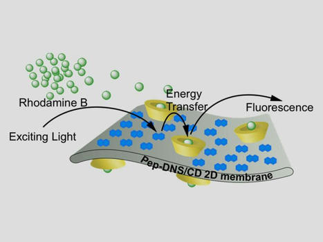
Inspired by nature, researchers at the Pacific Northwest National Laboratory (PNNL), along with collaborators from Washington State University, created a novel material capable of capturing light energy. This material provides a highly efficient artificial light-harvesting system with potential applications in photovoltaics and bioimaging.
The research provides a foundation for overcoming the difficult challenges involved in the creation of hierarchical functional organic-inorganic hybrid materials. Nature provides beautiful examples of hierarchically structured hybrid materials such as bones and teeth. These materials typically showcase a precise atomic arrangement that allows them to achieve many exceptional properties, such as increased strength and toughness.
PNNL materials scientist Chun-Long Chen, corresponding author of this study, and his collaborators created a new material that reflects the structural and functional complexity of natural hybrid materials. This material combines the programmability of a protein-like synthetic molecule with the complexity of a silicate-based nanocluster to create a new class of highly robust nanocrystals. They then programmed this 2D hybrid material to create a highly efficient artificial light-harvesting system.
“The sun is the most important energy source we have,” said Chen. “We wanted to see if we could program our hybrid nanocrystals to harvest light energy—much like natural plants and photosynthetic bacteria can—while achieving a high robustness and processibility seen in synthetic systems.” The results of this study were published May 14, 2021, in Science Advances.
Catastrophic collapse of materials and structures is the inevitable consequence of a chain reaction of locally confined damage - from solid ceramics that snap after the development of a small crack to metal space trusses that give way after the warping of a single strut. In a study published recently in Advanced Materials, engineers at the University of California, Irvine and the Georgia Institute of Technology describe the creation of a new class of mechanical metamaterials that delocalize deformations to prevent failure. They did so by turning to tensegrity, a century-old design principle in which isolated rigid bars are integrated into a flexible mesh of tethers to produce very lightweight, self-tensioning truss structures. Starting with 950 nanometer-diameter members, the team used a sophisticated direct laser writing technique to generate elementary cells sized between 10 and 20 microns. These were built up into eight-unit supercells that could be assembled with others to make a continuous structure. The researchers then conducted computational modeling and laboratory experiments and observed that the constructs exhibited uniquely homogenous deformation behavior free from localized overstress or underuse. The team showed that the new metamaterials feature a 25-fold enhancement in deformability and an orders-of-magnitude increase in energy absorption over state-of-the-art lattice arrangements. "Tensegrity structures have been studied for decades, particularly in the context of architectural design, and they have recently been found in a number of biological systems," said senior co-author Lorenzo Valdevit, a UCI professor of materials science and engineering who directs the Architected Materials Group. "Proper periodic tensegrity lattices were theoretically conceptualized only a few years ago by our co-author Julian Rimoli at Georgia Tech, but through this project we have achieved the first physical implementation and performance demonstration of these metamaterials."
Gasoline and diesel engines, which are powered by fossil fuels, will soon be sidelined by climate change. Instead, new propulsion systems will be required. One fuel with a big potential is hydrogen. Hydrogen vehicles are equipped with a reinforced tank that is fueled at a pressure of 700 bar. This tank feeds a fuel cell, which converts the hydrogen into electricity. This in turn drives an electric motor to propel the vehicle. In the case of passenger cars, this technology is well advanced, with several hundred hydrogen-powered automobiles already in operation on German roads. At the same time, the network of hydrogen stations in Germany is projected to grow from 100 to 400 over the next three years. Yet hydrogen is not currently an option for small vehicles such as electric scooters and motorcycles, since the pressure surge during refilling would be too great. However, researchers from the Fraunhofer Institute for Manufacturing Technology and Advanced Materials IFAM in Dresden have now come up with a hydrogen-based fuel that is ideal for small vehicles: Powerpaste, which is based on solid magnesium hydride. “Powerpaste stores hydrogen in a chemical form at room temperature and atmospheric pressure to be then released on demand,” explains Dr. Marcus Vogt, research associate at Fraunhofer IFAM. And given that Powerpaste only begins to decompose at temperatures of around 250 °C, it remains safe even when an e-scooter stands in the baking sun for hours. Moreover, refueling is extremely simple. Instead of heading to the filling station, riders merely have to replace an empty cartridge with a new one and then refill a tank with mains water. This can be done either at home or underway. The starting material of Powerpaste is magnesium, one of the most abundant elements and, therefore, an easily available raw material. Onboard the vehicle, the Powerpaste is released from a cartridge by means of a plunger. When water is added from an onboard tank, the ensuing reaction generates hydrogen gas in a quantity dynamically adjusted to the actual requirements of the fuel cell. In fact, only half of the hydrogen originates from the Powerpaste ; the rest comes from the added water. “Powerpaste thus has a huge energy storage density,” says Vogt. “It is substantially higher than that of a 700 bar high-pressure tank. And compared to batteries, it has ten times the energy storage density.” This means that Powerpaste offers a range comparable to – or even greater than – gasoline. And it also provides a higher range than compressed hydrogen at a pressure of 700 bar.
Via Sepp Hasslberger
Researchers at the University of Manchester in the UK have identified a new family of quasiparticles in superlattices made from graphene sandwiched between two slabs of boron nitride. The work is important for fundamental studies of condensed-matter physics and could also lead to the development of improved transistors capable of operating at higher frequencies. In recent years, physicists and materials scientists have been studying ways to use the weak (van der Waals) coupling between atomically thin layers of different crystals to create new materials in which electronic properties can be manipulated without chemical doping. The most famous example is graphene (a sheet of carbon just one atom thick) encapsulated between another 2D material, hexagonal boron nitride (hBN), which has a similar lattice constant. Since both materials also have similar hexagonal structures, regular moiré patterns (or “superlattices”) form when the two lattices are overlaid. If the stacked layers of graphene-hBN are then twisted, and the angle between the two materials’ lattices decreases, the size of the superlattice increases. This causes electronic band gaps to develop through the formation of additional Bloch bands in the superlattice’s Brillouin zone (a mathematical construct that describes the fundamental ideas of electronic energy bands). In these Bloch bands, electrons move in a periodic electric potential that matches the lattice and do not interact with one another. Hofstadter’s butterfly In 2013, the Manchester team led by Andrei Geim and Alexey Berdyugin, along with two independent groups at the Massachusetts Institute of Technology and Columbia University in the US, observed a stunning fractal pattern in plots of electron density versus magnetic field strength in these graphene-hBN superlattices. This pattern, known as “Hofstadter’s butterfly”, emerged when the teams determined the energy spectrum of the superlattices by measuring their electrical conductivity in strong magnetic fields of up to 17 Tesla. The Manchester researchers now report another surprising behavior of electrons in such structures, again under strong magnetic fields. “It is well known that in a zero magnetic field, electrons move in straight trajectories and if you apply a magnetic field they start to bend and move in circles, which decreases the conductivity,” explain team members Julien Barrier and Piranavan Kumaravadivel, who carried out the experimental work. “In a graphene layer aligned with hBN, electrons also start to bend, but if you set the magnetic field at specific values, the conductivity increases sharply. It is as if the electrons moved in straight line trajectories again, like in a metal with no magnetic field anymore.”
Nanostructured layers boast countless potential properties -- but how can the most suitable one be identified without any long-term experiments? A team has ventured a shortcut: using a machine learning algorithm, the researchers were able to reliably predict the properties of such a layer. Porous or dense, columns or fibers During the manufacture of thin films, numerous control variables determine the condition of the surface and, consequently, its properties. Relevant factors include the composition of the layer as well as process conditions during its formation, such as temperature. All these elements put together result in the creation of either a porous or a dense layer during the coating process, with atoms combining to form columns or fibers. "In order to find the optimal parameters for an application, it used to be necessary to conduct countless experiments under different conditions and with different compositions; this is an incredibly complex process," explains Professor Alfred Ludwig, Head of the Materials Discovery and Interfaces Team. Findings yielded by such experiments are so-called structure zone diagrams, from which the surface of a certain composition resulting from certain process parameters can be read. "Experienced researchers can subsequently use such a diagram to identify the most suitable location for an application and derive the parameters necessary for producing the suitable layer," points out Ludwig. "The entire process requires an enormous effort and is highly time consuming." Algorithm predicts surface Striving to find a shortcut towards the optimal material, the team took advantage of artificial intelligence, more precisely machine learning. To this end, PhD researcher Lars Banko, together with colleagues from the Interdisciplinary Centre for Advanced Materials Simulation at RUB, Icams for short, modified a so-called generative model. He then trained this algorithm to generate images of the surface of a thoroughly researched model layer of aluminum, chromium and nitrogen using specific process parameters, in order to predict what the layer would look like under the respective conditions. "We fed the algorithm with a sufficient amount of experimental data in order to train it, but not with all known data," stresses Lars Banko. Thus, the researchers were able to compare the results of the calculations with those of the experiments and analyze how reliable its prediction was. The results were conclusive: "We combined five parameters and were able to look in five directions simultaneously using the algorithm -- without having to conduct any experiments at all," outlines Alfred Ludwig. "We have thus shown that machine learning methods can be transferred to materials research and can help to develop new materials for specific purposes."
A magnetic atom epitomizes the scaling limit for magnetic information storage. Individual atomic spins have recently exhibited magnetic remanence, a requirement for magnetic memory. However, such memory has been only realized on thin insulating surfaces. Black phosphorus (BP) has recently gained substantial momentum within the fields of physics, electronics and optoelectronics because of its layer-dependent band gap spanning the visible spectrum, high carrier mobility, and field-tunable band topology. While black phosphorus devices gain sophistication and performance at remarkable speeds, the atomic scale properties remain largely unexplored. Using atomic scale probes, scientists have recently been able to classify, characterize, and quantify the primary native defects in BP, namely P vacancies. They have further shown that such vacancies host electronic states near the valence band edge, acting a p-type dopants and serve as scattering centers for free carriers. The interactions and arrangements of alkali metal dopants on the surface of BP have revealed a complex distance dependent electrostatic screening mediated by strongly confined 2D states at the BP surface. A peculiar case is the single cobalt atom (extrinsic defect) on the surface of black phosphorus. Screening from the black phosphorus enables these magnetic atoms to stabilize multiple orbital configurations (3d8 and 3d9) allowing us to demonstrate a proof-of-concept single atom magnetic memory.
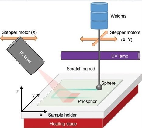
Mechanoluminescence (ML) is a type of luminescence induced by any mechanical action on a solid, leading to a range of applications in materials research, photonics and optics. For instance, the mechanical action can release energy previously stored in the crystal lattice of phosphor via trapped charge carriers. However, the method has limits when recording ML emissions during a pressure-induced event. In a new study, Robin R. Petit and a research team at the LumiLab, Department of Solid State Sciences at the Ghent University—Belgium devised a new technique to add a memory function to pressure-sensitive phosphors. Using the method, the scientists obtained an optical readout of the location and intensity of a pressure event three days (72 hours) after the event. The team noted the outcome using Europium-doped barium silicon oxynitride (BaSiO2N2:Eu2+) phosphor, which contained a broad trap depth distribution or depth of defect distribution—essential for the unique memory function. The excited electrons of phosphor filled the 'traps' (or defects) in the crystal lattice, which could be emptied by applying weight to emit light. The research team merged optically stimulated luminescence (OSL), thermoluminescence (TL) and ML measurements to carefully analyze the influence of light, heat and pressure on trap depth distribution. Based on the memory effect, the materials remembered the location at which pressure had occurred, helping researchers to develop new pressure sensing applications and study charge carrier transitions within energy storage phosphors. The work is now published on Light: Science & Applications. When specific materials are subjected to mechanical action, light emission can be observed as mechanoluminescence (ML). The process can be induced through different types of mechanical stress including friction, fracture, bending, impact of a weight and even ultrasound, crystallization and wind. The phenomenon can be used to identify stress distribution, microcrack propagation and structural damages in solids, while allowing a variety of applications in displays, to visualize ultrasound and even map personalized handwriting. However, the technique is limited by the range of emission colors, restriction of real-time measurements and restricted signal visibility.
A team of researchers at McMaster University has developed a self-cleaning surface that can repel all forms of bacteria, preventing the transfer of antibiotic-resistant superbugs and other dangerous bacteria in settings ranging from hospitals to kitchens. The new plastic surface – a treated form of conventional transparent wrap – can be shrink-wrapped onto door handles, railings, IV stands and other surfaces that can be magnets for bacteria such as MRSA and C. difficile. The treated material is also ideal for food packaging, where it could stop the accidental transfer of bacteria such as E. coli, Salmonella and listeria from raw chicken, meat and other foods, as described in a paper published today by the journal ACS Nano. The research was led by engineers Leyla Soleymani and Tohid Didar, who collaborated with colleagues from McMaster’s Institute for Infectious Disease Research and the McMaster-based Canadian Centre for Electron Microscopy. Inspired by the water-repellent lotus leaf, the new surface works through a combination of nano-scale surface engineering and chemistry. The surface is textured with microscopic wrinkles that exclude all external molecules. A drop of water or blood, for example, simply bounces away when it lands on the surface. The same is true for bacteria.
Engineers find that limpets' tiny teeth are made of the strongest biological material ever tested. Limpets cling tenaciously to rocks as waves batter them. They can clamp on with a force of 75 pounds per square inch, using their muscular mollusk "foot" and a chemical secretion. But even that feat isn’t as stunning as their ability to grind down rock as they feed, using a tooth-studded tongue called a radula. Now the snails have upped their tough-guy street cred with help from engineers based in the U.K., who discovered that these snails’ teeth are made of the strongest natural material out there. Spider silk, often compared to kevlar, has wowed with its tough yet flexible powers. But when tested, the tooth material was, on average, about five times stronger than most spider silk, reports BBC News. This makes it the strongest natural material on Earth. Tests in the lab revealed that it can withstand pressure that would turn carbon into diamond. Thats’s comparable to a single strand of spaghetti holding up about 3,300 one-pound bags of sugar, the study’s lead author, Asa Barber of the University of Portsmouth, told the BBC.
Researchers, inspired by diving bell spiders and rafts of fire ants, have created a metallic structure that is so water repellent, it refuses to sink—no matter how often it is forced into water or how much it is damaged or punctured. Could this lead to an unsinkable ship? A wearable flotation device that will still float after being punctured? Electronic monitoring devices that can survive in long term in the ocean? All of the above, says Chunlei Guo, professor of optics and physics, whose lab describes the structure in ACS Applied Materials and Interfaces .The structure uses a groundbreaking technique the lab developed for using femtosecond bursts of lasers to “etch” the surfaces of metals with intricate micro- and nanoscale patterns that trap air and make the surfaces superhydrophobic, or water repellent.
Researchers at the University of California, Irvine have developed a new scanning transmission electron microscopy method that enables visualization of the electric charge density of materials at sub-angstrom resolution. With this technique, the UCI scientists were able to observe electron distribution between atoms and molecules and uncover clues to the origins of ferroelectricity, the capacity of certain crystals to possess spontaneous electric polarization that can be switched by the application of an electric field. The research, which is highlighted in a study published today in Nature, also revealed the mechanism of charge transfer between two materials. "This method is an advancement in electron microscopy—from detecting atoms to imaging electrons—that could help us engineer new materials with desired properties and functionalities for devices used in data storage, energy conversion and quantum computing," said team leader Xiaoqing Pan, UCI's Henry Samueli Endowed Chair in Engineering and a professor of both materials science & engineering and physics & astronomy. Employing a new aberration-corrected scanning transmission electron microscope with a fine electron probe measuring half an angstrom and a fast-direct electron detection camera, his group was able to acquire a 2-D raster image of diffraction patterns from a region of interest in the sample. As obtained, the data sets are 4-D, since they consist of 2-D diffraction patterns from each probe location in a 2-D scanning area. "With our new microscope, we can routinely form an electron probe as small as 0.6 angstrom, and our high-speed camera with angular resolution can acquire 4-D STEM images with 512 x 512 pixels at greater than 300 frames per second," Pan said. "Using this technique, we can see the electron charge distribution between atoms in two different perovskite oxides, non-polar strontium titanate and ferroelectric bismuth ferrite."
Researchers show, for the first time, the ability to globally align single-wall carbon nanotubes along a common axis. A University of Wyoming researcher and his team have shown, for the first time, the ability to globally align single-wall carbon nanotubes along a common axis. This discovery can be valuable in many areas of technology, such as electronics, optics, composite materials, nanotechnology and other applications of materials science. “Unlike previous efforts to align nanotubes using nanotube solution filtration, we created an automated system that could create multiple aligned films at one time,” says William Rice, an assistant professor in UW’s Department of Physics and Astronomy. “Automating the filtration system also had the effect that we could precisely control the filtration flow rate, which produced higher alignment.” Rice was corresponding author of a paper, titled “Global Alignment of Solution-Based, Single-Wall Carbon Nanotube Films via Machine-Vision Controlled Filtration,” which was published in Nano Letters ("Global Alignment of Solution-Based Single-Wall Carbon Nanotube Films via Machine-Vision Controlled Filtration").
|
Changing climate patterns have left millions of people vulnerable to weather extremes. As temperature fluctuations become more commonplace around the world, conventional power-guzzling cooling and heating systems need a more innovative, energy-efficient alternative, and in turn, lessen the burden on already struggling power grids. In a new study, researchers at Texas A&M University have created novel 3D printable phase-change material (PCM) composites that can regulate ambient temperatures inside buildings using a simpler and cost-effective manufacturing process. Furthermore, these composites can be added to building materials, like paint, or 3D printed as decorative home accents to seamlessly integrate into different indoor environments. "The ability to integrate phase-change materials into building materials using a scalable method opens opportunities to produce more passive temperature regulation in both new builds and already existing structures," said Dr. Emily Pentzer, associate professor in the Department of Materials Science and Engineering and the Department of Chemistry. Dr. Emily Pentzer and her team have created novel 3D printable phase-change material composites that can regulate ambient temperatures inside buildings using a simpler and cost-effective manufacturing process. This study was published in the June issue of the journal Matter. Heating, ventilation and air conditioning (HVAC) systems are the most commonly used methods to regulate temperatures in residential and commercial establishments. However, these systems guzzle a lot of energy. Furthermore, they use greenhouse materials, called refrigerants, for generating cool, dry air. These ongoing issues with HVAC systems have triggered research into alternative materials and technologies that require less energy to function and can regulate temperature commensurate to HVAC systems. One of the materials that have gained a lot of interest for temperature regulation is phase-change materials. As the name suggests, these compounds change their physical state depending on the temperature in the environment. So, when phase-change materials store heat, they convert from solid to liquid upon absorbing heat and vice versa when they release heat. Thus, unlike HVAC systems that rely solely on external power to heat and cool, these materials are passive components, requiring no external electricity to regulate temperature.
To really appreciate what a team of researchers led by Maksym Kovalenko and Maryna Bodnarchuk has achieved, it is best to start with something mundane: Crystals of table salt are familiar to anyone who has ever had to spice up an overtly bland lunch. Sodium chloride -- NaCl in chemical terms -- is the name of the helpful chemical; it consists of positively charged sodium ions (Na+) and negatively charged chloride ions (Cl-). You can imagine the ions as beads that strongly attract each other forming densely packed and rigid crystals like the ones we can see in a saltshaker. Many naturally occurring minerals consist of ions -- positive metal ions and negative ions, which arrange themselves into different crystal structures depending on their relative sizes. In addition, there are structures such as diamond and silicon: These crystals consist of only one kind of atoms -- carbon in the case of diamond -, but, similar to minerals, the atoms are also held together by strong bonding forces. What if all strong bonding forces between atoms could be eliminated? In the realm of atoms, with all the quantum mechanics at play, this would not yield a molecule or a solid-state matter, at least at ambient conditions. "But modern chemistry can produce alternative building blocks that can indeed have vastly different interactions than those between atoms," says Maksym Kovalenko, Empa researcher and professor of chemistry at ETH Zurich. "They can be as hard as billiard balls in a sense that they sense each other only when colliding. Or they can be softer on the surfaces, like tennis balls. Moreover, they can be built in many different shapes: not just spheres, but also cubes or other polyhedra, or more anisotropic entities." Such building blocks are made of hundreds or thousands of atoms and are known as inorganic nanocrystals. Kovalenko's team of chemists at Empa and ETH is able to synthesize them in large quantities with a high degree of uniformity. Kovalenko and Bodnarchuk, and some of their colleagues the world over, have been working for about 20 years now with these kinds of building blocks. The scientists call them "Lego materials" because they form long-range ordered dense lattices known as superlattices. It had long been speculated that mixing different kinds of nanocrystals would allow the engineering of completely new supramolecular structures. The electronic, optical or magnetic properties of such multicomponent assemblies would be expected to be a mélange of the properties of the individual components. In the early years, the work had focused on mixing spheres of different sizes, resulting in dozens of various superlattices with packing structures that mimic common crystal structures, such as table salt -- albeit with crystal unit cells ten- to 100-times larger. With their latest article in "Nature," the team led by Kovalenko and Bodnarchuk now managed to expand the knowledge a great deal further: They set out to study a mixture of different shapes -- spheres and cubes to start with. This seemingly simple deviation from the mainstream immediately led to vastly different observations. Moreover, the chosen cubes, namely colloidal cesium lead halide perovskite nanocrystals, are known as some of the brightest light emitters developed to date, ever since their invention by the same team six years ago. The superlattices the researchers obtained are not only peculiar as far as their structure is concerned, but also with respect to some of their properties. In particular, they exhibit superfluorescence -- that is, the light is irradiated in a collective manner and much faster than the same nanocrystals can accomplish in their conventional state, embedded in a liquid or a powder.
USC researchers harness the power of living organisms to make materials that are strong, tolerant and resilient. Biological systems can harness their living cells for growth and regeneration, but engineering systems cannot. Until now. Qiming Wang and researchers at the USC Viterbi School of Engineering are harnessing living bacteria to create engineering materials that are strong, tolerant, and resilient. The research is published in Advanced Materials. “The materials we are making are living and self-growing,” said Wang, the Stephen Schrank Early Career Chair in Civil and Environmental Engineering and assistant professor of civil and environmental engineering in the Sonny Astani Department of Civil and Environmental Engineering (CEE). “We have been amazed by the sophisticated microstructures of natural materials for centuries, especially after microscopes were invented to observe these tiny structures. Now we take an important step forward: We use living bacteria as a tool to directly grow amazing structures that cannot be made on our own.” The researchers work with specific bacteria— S. pasteurii—known for secreting an enzyme called urease. When urease is exposed to urea and calcium ions, it produces calcium carbonate, a fundamental and strong mineral compound found in bones or teeth. “The key innovation in our research,” said Wang, “is that we guide the bacteria to grow calcium carbonate minerals to achieve ordered microstructures which are similar to those in the natural mineralized composites.” Wang added: “Bacteria know how to save time and energy to do things. They have their own intelligence, and we can harness their smartness to design hybrid materials that are superior to fully synthetic options. Borrowing inspiration from nature is not new in engineering. As one would suspect, nature has great examples of complex mineralized composites that are strong, fracture resistant, and energy damping—for example nacre or the hard shell surrounding a mollusk. Wang said: “Although microorganisms such as bacteria, fungi and viri are sometimes detrimental in causing diseases—like COVID-19—they can also be beneficial. We have a long history of using microorganisms as factories—for example, using yeast to make beer. But there is limited research on using microorganisms to manufacture engineering materials.” Combining living bacteria and synthetic materials, Wang said this new living material demonstrates mechanical properties superior to that of any natural or synthetic material currently in use. This is largely due to the material’s bouligand structure, which is characterized by multiple layers of minerals laid at varying angles from each other to form a sort of “twist” or helicoidal shape. This structure is difficult to create synthetically.
As light as possible and as strong as possible at the same time. These are the requirements for modern lightweight materials, such as those used in aircraft construction and the automotive industry. A research team has now developed a new materials' design approach for future ultralight materials: Nanometer-sized metal struts that form nested networks on separate hierarchical levels provide amazing strength. When the Eiffel Tower was inaugurated in 1889, it was considered a technical marvel. Its artful and delicate arrangement of large and small iron girders provided extraordinary stability and made sure it became the world's tallest building at the time by a long shot. "Hierarchical" is what experts call the engineering approach of an open array of larger beams braced by smaller ones. For several years now, material science researchers have tried to transfer this efficient approach to the internal microstructure of materials, for example by using 3D printers that can replicate engineering truss structures on a micrometer scale. So far, hopes of creating a new generation of extremely strong lightweight construction materials have not been fulfilled. One of the reasons: "A 3D printer can only print a maximum of roughly ten thousand beams and that will take hours," according to Professor Jörg Weißmüller of the Institute of Materials Mechanics at HZG, co-author of the current publication. "For practical applications, this is not really a viable option." Corroding away silver Nevertheless, his team is pursuing an even more ambitious goal. The vision: If beams could be strengthened by downsizing to few nanometers in diameter, they could provide the basis for a new type of material -- exceptionally light and at the same time strong. However, this kind of material would have to contain trillions of beams, far exceeding the capability of even the most sophisticated printer. "That is why we have to trick nature into making these kinds of materials for us, simply by self-organization," Weißmüller's colleague Dr. Shan Shi, lead author of the study, explains. As a start, the team used an alloy of 93% silver and 7% gold. This alloy is dipped into diluted sulfuric acid, dissolving out approximately half of the silver. As a result, the remaining material rearranges itself, forming a delicate network of nanoscale beams. Afterwards, the material undergoes a heat treatment at several hundred degrees. "This coarsens the network to a beam size of 150 nanometers while maintaining the original architecture," Shi explains. During the last step, acid comes into play once again. It is used to wash out the rest of the silver, leaving only gold beams with a pore size of 15 nanometers on average. The result is a hierarchically structured material with two distinctly different beam sizes, not unlike the Eiffel Tower. As a result of its open network structure, this new material consists of 80 to 90% air, giving it a density of only 10 to 20% of the solid metal.
Researchers at Princeton University in the US have become the first to observe a robust supercurrent at the edge of a superconductor that is very different to the supercurrent in the material’s bulk. This “topological superconductivity” could come in useful for a host of new applications, they say. Topological materials are materials that have very different properties at the surface compared to those in their bulk thanks to special topologically protected “edge states”. Topological insulators – materials that act as insulators in their interior but conduct currents on their surface – have been a hot topic in condensed-matter research for several years, but their superconducting counterparts are less well-studied. To find out what happens when the interior of a topological material is not an insulator but a superconductor, Nai Phuan Ong and colleagues turned their attention to molybdenum ditelluride (MoTe2). This material is a Weyl semimetal, a recently discovered class of topological material in which electrons (which are fermions, and thus have spin-1/2) behave as if they have no mass. These oddly-behaved particles were predicted in 1929 by theoretical physicist Herman Weyl as a solution to the Dirac equation (which describes the physics of normal fermions), and they travel faster and dissipate less energy than electrons in ordinary metals or semiconductors. They also show the “chiral magnetic effect” when placed in a magnetic field, which generates a current of positive and negative Weyl particles that move parallel and antiparallel to the field. Saw-tooth pattern in critical current oscillations The researchers began by preparing slivers of crystals of MoTe2 that were between 60 to 120 nm thick. They then cooled these crystalline samples down to below 100 millikelvin – the superconducting transition temperature of MoTe2. Next, they applied a weak magnetic field to the samples while measuring the current flow through them. The Princeton team observed a quantity known as the critical current oscillating in a saw-tooth pattern as they increase the applied magnetic field. Both the height and frequency of these oscillations fit well with predictions of how these fluctuations arise from the quantum behavior of electrons confined to the edges of the material, they say. In superconducting materials, electrons overcome their mutual electrostatic repulsion to form Cooper pairs thanks to interactions between the electrons and vibrations of the material’s crystalline lattice. Once formed, these pairs behave as bosons, which have an integer spin. This means they can condense to form a “superfluid” state that behaves as a single entity, carrying electrical current through the material with no resistance at temperatures below the material’s transition temperature.
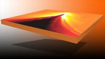
Since the late 19th century, scientists have understood that, when heated, all materials emit light in a predictable spectrum of wavelengths. Research published today in Nature Scientific Reports presents a material that emits light when heated that appears to exceed the limits set by that natural law. Could there be a new kind of light in the universe? Since the late 19th century, scientists have understood that, when heated, all materials emit light in a predictable spectrum of wavelengths. Research published today in Nature Scientific Reports presents a material that emits light when heated that appears to exceed the limits set by that natural law. In 1900, Max Planck first mathematically described a pattern of radiation and ushered in the quantum era with the assumption that energy can only exist in discrete values. Just as a fireplace poker glows red hot, increasing heat causes all materials to emit more intense radiation, with the peak of the emitted spectrum shifting to longer wavelengths as heat rises. In keeping with Planck's Law, nothing can emit more radiation than a hypothetical object that absorbs energy perfectly, a so-called "blackbody." The new material discovered by Shawn Yu Lin, lead author and a professor of physics at Rensselaer Polytechnic Institute, defies the limits of Planck's law, emitting a coherent light similar to that produced by lasers or LEDs, but without the costly structure needed to produce the stimulated emission of those technologies. In addition to the spectroscopy study just published in Nature Scientific Reports, Lin previously published an imaging study in IEEE Photonics Journal. Both show a spike in radiation at about 1.7 microns, which is the near-infrared portion of the electromagnetic spectrum. "These two papers offer the most convincing evidence of 'super-Planckian' radiation in the far-field," said Lin. "This doesn't violate Planck's law. It's a new way to generate thermal emission, a new underlying principle. This material, and the method that it represents, opens a new path to realize super-intense, tunable LED-like infrared emitters for thermophotovoltaics and efficient energy applications." For his research, Lin built a three-dimensional tungsten photonic crystal -- a material that can control the properties of a photon -- with six offset layers, in a configuration similar to a diamond crystal, and topped with an optical cavity that further refines the light. The photonic crystal shrinks the spectrum of light that is emitted from the material to a span of about 1 micrometer. The cavity continues to squeeze the energy into a span of roughly 0.07 micrometers. Lin has been working to establish this advance for 17 years, since he created the first all-metallic photonic crystal in 2002, and the two papers represent the most rigorous tests he has conducted. "Experimentally, this is very solid, and as an experimentalist, I stand by my data. From a theoretical perspective, no one yet has a theory to fully explain my discovery," Lin said.
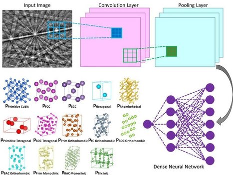
Nanoengineers at the University of California San Diego have developed a computer-based method that could make it less labor-intensive to determine the crystal structures of various materials and molecules, including alloys, proteins and pharmaceuticals. The method uses a machine learning algorithm, similar to the type used in facial recognition and self-driving cars, to independently analyze electron diffraction patterns, and do so with at least 95% accuracy. The work is published in the Jan. 31 issue of Science. A team led by UC San Diego nanoengineering professor Kenneth Vecchio and his Ph.D. student Kevin Kaufmann, who is the first author of the paper, developed the new approach. Their method involves using a scanning electron microscope (SEM) to collect electron backscatter diffraction (EBSD) patterns. Compared to other electron diffraction techniques, such as those in transmission electron microscopy (TEM), SEM-based EBSD can be performed on large samples and analyzed at multiple length scales. This provides local sub-micron information mapped to centimeter scales. For example, a modern EBSD system enables determination of fine-scale grain structures, crystal orientations, relative residual stress or strain, and other information in a single scan of the sample. However, the drawback of commercial EBSD systems is the software's inability to determine the atomic structure of the crystalline lattices present within the material being analyzed. This means a user of the commercial software must select up to five crystal structures presumed to be in the sample and then the software attempts to find probable matches to the diffraction pattern. The complex nature of the diffraction pattern often causes the software to find false structure matches in the user selected list. As a result, the accuracy of the existing software's determination of the lattice type is dependent on the operator's experience and prior knowledge of their sample. The method that Vecchio's team developed does this all autonomously, as the deep neural network independently analyzes each diffraction pattern to determine the crystal lattice, out of all possible lattice structure types, with a high degree of accuracy (greater than 95%).
Researchers from NUS have synthesized the world’s first one-atom-thick amorphous material. Previously thought to be impossible, the discovery of monolayer amorphous carbon (MAC) could finally settle a decades-old debate of exactly how atoms are arranged in amorphous solids, and open up potential applications. This major research breakthrough was led by Professor Barbaros Özyilmaz, Head of the NUS Materials Science and Engineering. The results were published in the prestigious scientific journal Nature on 8 January 2020. The NUS team grew the material and studied its properties and potential areas of application. In addition, atomic resolution imaging was performed by the group of Professor Kazu Suenaga from the National Institute of Advanced Industrial Science and Technology (AIST), Japan, and Professor Junhao Lin from Southern University of Science and Technology (SUSTECH), China. Furthermore, theoretical simulations were carried out by the group of Professor Sokrates Pantelides from Vanderbilt University, USA. “With MAC, we have shown for the first time that fully amorphous materials can be stable and free-standing in single atomic layers. Amorphous materials are of great technological importance, but surprisingly, they remain poorly understood from a basic science point of view. This breakthrough allows for direct imaging to reveal how atoms are arranged in amorphous materials, and could be of commercial value for batteries, semiconductors, membranes and many more applications,” said Prof Özyilmaz, who is also from NUS Physics and the NUS Centre for Advanced 2D Materials.
A new study proposed a scheme to achieve ultrahigh reduced transition temperature, up to Tc/TF ~ 1, in two-component atomic Fermi gases, a system that mimic high Tc superconductors, via a tunable pairing interaction strength, using mixed dimensions where one component is in a deep one-dimensional (1D) optical lattice with a large lattice spacing, while the other remains in 3D free space. Quantum atomic Fermi gases have provided an ideal prototype for studying the physics of high Tc superconductivity, including the underlying pairing mechanism and the unusual pseudogap phenomena, which have been at the heart of debate in the field of high Tc superconductivity.
In a Letter published in SCIENCE CHINA Physics, Mechanics & Astronomy, theorists from Zhejiang University, Sun Yat-Sen University, and Zhejiang University of Technology, as well as the Synergetic Innovation Center of Quantum Information and Quantum Physics, report that by tuning the lattice spacing to be large in a mixed dimensional setting, the reduced superfluid transition temperature, Tc/TF, can be made extremely high, higher than that for any known systems.
It has been a long-term goal in the field of superconductivity to achieve a high transition temperature Tc, ideally up to room temperature (about 300 K) and above. Given that the typical electron kinetic energy, represented by its Fermi temperature TF, is of the order of 10000 K in a solid, this is only a small fraction. Conventional superconductors in metals and alloys have a transition temperature of a few Kelvins, usually below 20 K. The high Tc cuprate superconductors, discovered in 1986, has a Tc up to 95 K at the optimal oxygen doping concentration under ambient pressure, and up to 164 K under high pressure, has a relatively low TF due to strong electron correlations, which pushes the reduced temperature Tc/TF up to about 0.05.
This ratio does not exceed this value for other families of superconductors, either, including iron-based superconductors, heavy fermion superconductors, organic superconductors, the monolayer FeSe/SrTiO3 superconductors, and the newly discovered magic angle twisted bilayer graphene, as well as the Tc record holder, H2S under high pressure. A higher ratio is made possible in ultracold atomic Fermi gases, with Tc/TF up to 0.218 in the BEC limit in the 3D homogeneous case. This ratio can be further raised to 0.518 in a harmonic trap in the BEC limit, utilizing the enhanced local Fermi energy at the trap center. This enhancement led to the idea of using mixed dimensions to tune the Fermi energy as a function of lattice spacing.
Atoms, molecules or even living cells can be manipulated with light beams. At TU Wien a method was developed to revolutionize such "optical tweezers". They are reminiscent of the "tractor beam" in Star Trek: Special light beams can be used to manipulate molecules or small biological particles. Even viruses or cells can be captured or moved. However, these optical tweezers only work with objects in empty space or in transparent liquids. Any disturbing environment would deflect the light waves and destroy the effect. This is a problem, in particular with biological samples because they are usually embedded in a very complex environment. But scientists at TU Wien (Vienna) have now shown how virtue can be made of necessity: A special calculation method was developed to determine the perfect wave form to manipulate small particles in the presence of a disordered environment. This makes it possible to hold, move or rotate individual particles inside a sample—even if they cannot be touched directly. The tailor-made light beam becomes a universal remote control for everything small. Microwave experiments have already demonstrated that the method works. The new optical tweezer technology has now been presented in the journal Nature Photonics. "Using laser beams to manipulate matter is nothing unusual anymore," explains Prof. Stefan Rotter from the Institute for Theoretical Physics at TU Wien. In 1997, the Nobel Prize in Physics was awarded for laser beams that cool atoms by slowing them down. In 2018, another Physics Nobel Prize recognized the development of optical tweezers. But light waves are sensitive: in a disordered, irregular environment, they can be deflected in a highly complicated way and scattered in all directions. A simple, plane light wave then becomes a complex, disordered wave pattern. This completely changes the way light interacts with a specific particle. "However, this scattering effect can be compensated," says Michael Horodynski, first author of the paper. "We can calculate how the wave has to be shaped initially so that the irregularities of the disordered environment transform it exactly into the shape we want it to be. In this case, the light wave looks rather disordered and chaotic at first, but the disordered environment turns it into something ordered. Countless small disturbances, which would normally render the experiment impossible, are used to generate exactly the desired wave form, which then acts on a specific particle.
Researchers have developed a tiny nanolaser that can fit and function inside of living tissues, such as deep-brain tissues, without harming them. Just 50 to 150 nanometers thick, the laser is about 1/1,000th the thickness of a single human hair. At this size, the laser can fit and function inside living tissues, with the potential to sense disease biomarkers or perhaps treat deep-brain neurological disorders, such as epilepsy. Developed by researchers at Northwestern and Columbia Universities, the nanolaser shows specific promise for imaging in living tissues. Not only is it made mostly of glass, which is intrinsically biocompatible, the laser can also be excited with longer wavelengths of light and emit at shorter wavelengths. "Longer wavelengths of light are needed for bioimaging because they can penetrate farther into tissues than visible wavelength photons," said Northwestern's Teri Odom, who co-led the research. "But shorter wavelengths of light are often desirable at those same deep areas. We have designed an optically clean system that can effectively deliver visible laser light at penetration depths accessible to longer wavelengths." The nanolaser also can operate in extremely confined spaces, including quantum circuits and microprocessors for ultra-fast and low-power electronics. The paper was published on Sept. 23, 2019 in the journal Nature Materials. Odom co-led the work with P. James Schuck at Columbia University's School of Engineering. While many applications require increasingly small lasers, researchers continually run into the same roadblock: Nanolasers tend to be much less efficient than their macroscopic counterparts. And these lasers typically need shorter wavelengths, such as ultraviolet light, to power them. "This is bad because the unconventional environments in which people want to use small lasers are highly susceptible to damage from UV light and the excess heat generated by inefficient operation," said Schuck, an associate professor of mechanical engineering. Odom, Schuck and their teams were able to achieve a nanolaser platform that solves these issues by using photon upconversion. In upconversion, low-energy photons are absorbed and converted into one photon with higher energy. In this project, the team started with low-energy, "bio-friendly" infrared photons and upconverted them to visible laser beams. The resulting laser can function under low powers and is vertically much smaller than the wavelength of light. "Our nanolaser is transparent but can generate visible photons when optically pumped with light our eyes cannot see," said Odom, the Charles E. and Emma H. Morrison Professor of Chemistry in Northwestern's Weinberg College of Arts and Sciences. "The continuous wave, low-power characteristics will open numerous new applications, especially in biological imaging."
A new scanning transmission electron microscopy technique developed by scientists from the University of California, Irvine allows the electric charge density of materials to be visualized at sub-angstrom resolution. The UCI researchers used this technique to view electron distribution between molecules and atoms and unravel clues to the roots of ferroelectricity. Ferroelectricity is the potential of specific crystals to exhibit spontaneous electric polarization that can be switched by applying an electric field. The study, which has been described in a research paper published recently in Nature, also demonstrated the charge transfer mechanism between two materials. “This method is an advancement in electron microscopy—from detecting atoms to imaging electrons—that could help us engineer new materials with desired properties and functionalities for devices used in data storage, energy conversion and quantum computing,” stated team leader Xiaoqing Pan, UCI’s Henry Samueli Endowed Chair in Engineering and a professor of both Materials Science & Engineering and Physics & Astronomy. His team used a new aberration-corrected scanning transmission electron microscope with a fine electron probe measuring half an angstrom and a fast direct electron detection camera to obtain a 2D raster image of diffraction patterns from an area of interest in the sample. When acquired, the data sets are 4D as they contain 2D diffraction patterns from each probe site in a 2D scanning area.
|