
Previous industry sources suggested that NVIDIA was exploring the use of Intel’s 18A process for its gaming GPUs, according to Tom’s Hardware. Now
Get Started for FREE
Sign up with Facebook Sign up with X
I don't have a Facebook or a X account


|
Scooped by
Richard Platt
onto Internet of Things - Company and Research Focus May 27, 12:44 AM
|
Previous industry sources suggested that NVIDIA was exploring the use of Intel’s 18A process for its gaming GPUs, according to Tom’s Hardware. Now

 Your new post is loading...
 Your new post is loading...
Your new post is loading...

SpaceX suffered a “major anomaly” as the the vehicle for its planned tenth Starship flight test exploded Wednesday night in Texas.
Richard Platt's insight:
Late Wednesday night at about 11PM CT, SpaceX was about to perform a static fire test of Ship 36, ahead of a planned 10th flight test for its Starship, when there was suddenly a massive explosion at the Massey’s Testing Center site. SpaceX says “A safety clear area around the site was maintained throughout the operation and all personnel are safe and accounted for,” and that there are no hazards to residents in the area of its recently incorporated town of Starbase, Texas. “After completing a single-engine static fire earlier this week, the vehicle was in the process of loading cryogenic propellant for a six-engine static fire when a sudden energetic event resulted in the complete loss of Starship and damage to the immediate area surrounding the stand,” according to an update on SpaceX’s website. “The explosion ignited several fires at the test site which remains clear of personnel and will be assessed once it has been determined to be safe to approach. Individuals should not attempt to approach the area while safing operations continue.”
Massive Data Breach Exposes 16 billion login Credentials including those related to Apple and Google
An incredible 16 billion login credentials, including those related to Apple, Google, Facebook, and more, are part of a massive data breach.
Richard Platt's insight:
An incredible 16 billion login credentials, including those related to Apple, Google, Facebook, and more, are part of a massive data breach.

Kevin Zhang, Deputy Co-Chief Operating Officer at TSMC, recently reiterated the company's cautious approach toward adopting High NA EUV lithography tools, emphasizing that TSMC is "in no rush" to bring the advanced technology into high-volume production. His remarks have reignited industry speculation around ASML's multi-billion-dollar next-generation lithography platform.
Richard Platt's insight:
Taiwan’s wafer foundry industry revenue is expected to rebound in the second quarter of 2025, with AI and HPC continuing to drive growth. However, tariff uncertainties may impact strategic deployment. Abstract - The revenue of Taiwan's foundry industry is expected to increase by 12.3% Q-on-Q to reach $31.42 billion in Q2 of 2025, driven by continued strong demand for AI and HPC chips, a rebound in handset-use application processor (AP) shipments, and the impact of US-China tariff effects, according to a DIGITIMES estimate. Notably, growth momentum may slow in Q3, 2025 due to the high base established in the Q2, 2025. However, the availability of new production capacity in advanced process nodes, price hikes, and increased inventory stocking due to tariff uncertainties are expected to continue supporting operational momentum. That said, rising geopolitical risks and continued uncertainty over US semiconductor tariff policies may impact the business deployment of Taiwan's wafer foundries.

From
sg

Globalfoundries was created by merging the former manufacturing operations of Advanced Micro Devices Inc with Singapore's Chartered Semiconductor
Richard Platt's insight:
GlobalFoundries Inc, the biggest US-based provider of made-to-order chips, announced a plan to spend US$16 billion to bolster domestic production. The company is budgeting US$13 billion to expand existing plants in New York and Vermont and making a further US$3 billion commitment to research into advanced packaging and other technologies in the US, GlobalFoundries is the latest company to publicly commit billions to increasing US production of electronics — announcements. GF said it’s making the investments with the endorsement of customers such as Apple Inc, Qualcomm Inc and General Motors Co. New CEO Tim Breen said GF isn’t providing a detailed breakdown of when the cash will be spent and will remain flexible in order to match supply with demand. The emphasis on the US is “a recognition of where there is the most unmet demand today,” GF says it’s carving out lucrative niches of the semiconductor industry. That includes an effort to combine chips with optical data components and an alternative material for power management chips, called gallium nitride (GaN). GlobalFoundries, is majority-owned by the government of Abu Dhabi, had previously been more conservative in its investment plans, saying it would only add capacity when supported by demand. On average, it’s spent about US$1.4 billion on new plants and equipment annually over the last 5 years. That’s a fraction of the multiple tens of billions that companies like Intel Corp and Samsung Electronics Co have spent. . Chip customers are looking for more local production and want to reduce dependence on suppliers that have their manufacturing concentrated in one location, Breen said. “Supply security matters,” he said. Requests for more production out of US plants have increased during the last six months. Globalfoundries, based in Malta, New York, manufactures so-called essential chips for semiconductor and electronics makers.
Such components don’t require the most advanced production, but they do handle vital tasks, such as controlling power and managing the flow of data inside devices. The AI boom also is increasing demand for a variety of chips. The GlobalFoundries investment is “a strategic response to the explosive growth in AI,”. The market has boosted the need for power-efficient and high-bandwidth chips used in Data Centers and communications equipment. Globalfoundries was created by merging the former manufacturing operations of AMD with Chartered Semiconductor — a deal that provided the new business with plants in the US, Germany and Singapore.
The company gave up on trying to compete with TSMC in the market for the most advanced production and has instead focused on cheaper techniques needed for other types of chips — components it says are becoming increasingly valuable.
Richard Platt's insight:
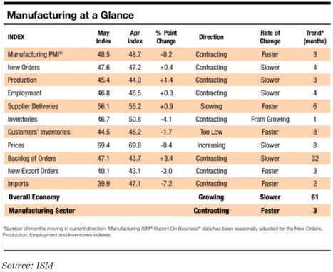
The report and respondent comments highlight an uncertain operating environment and the negative impacts of trade policies. Supply executives reported a “continued softening of demand” due to “higher prices and economic uncertainty.” The “impact of the current administration’s ever-changing trade policies has wreaked havoc on suppliers’ ability to react and remain profitable.” Some suppliers simply pass tariff costs directly on to customers. Uncertainty surrounding tariffs creates “supply chain disruptions rivaling that of COVID-19,” raising costs, impacting international orders, and forcing companies to undertake extensive and distracting contingency planning without clear direction. “With the uncertainty, manufacturers need to figure out and forecast profitability based on the cost of materials. (BOM - Bill of Materials Costs) It can be frustrating to have to do it multiple times a month or quarter. Lately, it’s been multiple times a week,” Susan Spence said in a conference call with reporters on Monday. “So, (the current situation) is not benefiting anybody right now, that’s for sure,” adding that navigating policy-driven challenges amid weakening demand will be crucial for the manufacturing sector.
Previous industry sources suggested that NVIDIA was exploring the use of Intel’s 18A process for its gaming GPUs, according to Tom’s Hardware. Now
Richard Platt's insight:
Previous industry sources suggested that NVIDIA was exploring the use of Intel’s 18A process for its gaming GPUs, according to Tom’s Hardware. Now, interest in the 18A node appears to be growing. Chosun Biz notes that Microsoft has reportedly signed a large-scale foundry deal with Intel using the 18A process, while talks with Google are also said to be underway. It's been noted that a Microsoft deal would mark a major milestone for Intel boosting its standing against TSMC and Samsung in advanced foundry. - Intel’s 18A process is currently in risk production and is expected to enter high volume manufacturing (HVM) late 2025. Intel is developing two enhanced variants of its 18A node: 18A-P, slated for launch in 2026, and 18A-PT, expected in 2028, it was noted that initial 18A-P wafers have already been introduced in Intel’s fabs. Intel is working with lead customers on its next-gen 14A node and started sharing early 14A PDKs with key partners. Chosun Biz notes that Intel has the largest number of U.S.-based factories among foundry players, potentially offering it an advantage in mitigating tariff-related risks. Intel is currently building 2 cutting-edge fabs in Arizona, alongside an expansion of its advanced packaging facilities in New Mexico. In Oregon, Intel is also moving forward with a new 300mm logic and foundry plant. In Ohio, it has committed USD 28 billion to construct 2 additional factories; but operations are now expected to begin between 2030 and 2032. Intel’s overseas expansion is picking up. in Ireland, HVM of the Intel 4 process is set to begin at Fab 34, with 3nm chip HVMN scheduled for later in 2025. In Israel, Fab 38 will produce HPC ICs using EUV lithography.
Intel Announced a Load of New Bugs Afflicting its ICs and & Not just CPUs but also GPUs are Involved
Richard Platt's insight:
Intel is notching up an impressive collection of bugs and flaws of late, crashing 13th and 14th Gen CPUs, the latest "Arrow Lake" chips needing a fair bit of post-launch work to get them running (not all that) optimally, all that good stuff. Now Intel has announced some exciting new bugs that afflict not just its CPUs, but also Arc GPUs. Let's start with some familiar sounding bugs involving Core Ultra processors. "Description: Incorrect initialization of resource in the branch prediction unit for some Intel Core Ultra Processors may allow an authenticated user to potentially enable information disclosure via local access," via the official security advisory. In other words, the bad guys can gain access to your rig. Intel says it is, "releasing microcode updates to mitigate these potential vulnerabilities," which impact Core Ultra 5, 7, and 9 CPU models across both desktop and laptop. The 2nd CPU bug afflicting those same chips is described as, "a potential security ['flaw'? Even Intel's bug reports have bugs, it seems...] in the Intel Integrated Connectivity I/O interface (CNVi) for some Intel Core Ultra Processors may allow escalation of privilege." A microcode fix is in the oven. In both cases, Intel advises that PC owners should contact their system provider for an update to fix the problem, but it's not clear if the fix has already been released by Intel. Next up, are novel GPU flaws, one of which has been given a "HIGH" severity by Intel. "Potential security vulnerabilities in some Intel Graphics Driver software may allow escalation of privilege, denial of service, or information disclosure,". This applies to all Intel iGPUs from 7th Gen CPUs onwards and also includes the latest Arc GPUs, like the Arc B580. And we have an advisory pertaining to Intel's Endurance Gaming Mode software. "A potential security vulnerability for some Endurance Gaming Mode software may allow escalation of privilege," Intel Endurance Gaming Mode is an app for laptops that monitors real-time frame rates. The idea is to keep power consumption in check by setting a target frame rate and then reducing GPU frequency and power to match, resulting in improved battery life. The fix for this is both an update to Endurance Gaming Mode version 1.5.651.0, available here, and that latest GPU driver we mentioned before, available here. All of which means if you have Intel laptop, say, with both the relevant CPU and GPU and you happen to use Endurance Gaming Mode, perhaps you'd better get patched up fast.

SMIC is reportedly trying to poach engineers to get Taiwanese semiconductor know how.
Richard Platt's insight:
Taiwan is investigating whether Semiconductor Manufacturing International Corp. (SMIC), China's largest contract chipmaker and the world's third largest foundry, broke local laws by secretly recruiting engineers to get experienced staff and gain insights of Taiwanese semiconductor know how, reports Bloomberg. The investigation is part of a broader crackdown on unauthorized activities by Chinese tech companies in Taiwan, notes Nikkei. Taiwanese authorities raided 34 different locations in 6 cities between March 18th - 28th. Officials from the Ministry of Justice examined operations linked to 11 Chinese companies and interviewed +90 people in connection with suspected breaches of local laws concerning talent poaching by Chinese companies. Most of the companies under investigation are involved in the semiconductor sector. Officials said this operation had been in the planning stages since December. Around 11 companies, the majority from the semiconductor industry, violated Taiwan's cross-strait regulations. Illegally setting up office without the government's knowledge. Of the 90 interviewees, some were witnesses, while others may have broken the law. The investigation revealed that SMIC used a company registered in Samoa to discreetly recruit engineers in Taiwan. Authorities also found that several other firms had formed unauthorized local entities to carry out hiring for work on advanced projects, including 'high-performance networking,' which is probably how business media describes silicon photonics, an area that is becoming increasingly important for next-generation AI and HPC datacenters. SMIC has 7nm-class and preps to roll-out 6nm-class process technologies, the best production nodes available in China. It produces chips for Huawei's HiSilicon, which tends to develop competitive offerings for client devices as well as AI servers and general-purpose servers. SMIC and Huawei need technologies like silicon photonics for their next-generation offerings. However, SMIC is not the only company that allegedly poaches engineers from Taiwanese companies. A company called Clounix was found to have poached a large number of specialists from major companies like Intel and Microsoft. It reportedly first disguised itself as a local company and later as a Singapore-based chip designer to avoid oversight. However, Clounix has financial backing from Ant Group, which is affiliated with Alibaba, which is emerging as a large cloud service provider with its own custom silicon division that develop CPUs and special-purpose ASICs for its broad needs, including general-purpose processing and AI workloads. Interestingly, Chinese entities were not only interested in advanced semiconductor or processor technologies know how. A company that develops display driver ICs has allegedly set up two offices in Tainan and Hsinchu and conducted remote interviews from China to bring in Taiwanese talent. It is unclear whether they wanted Taiwanese engineers to develop DDICs in China.

Intel expects its loss-making Foundry division to reach breakeven by 2027, driven by internal adoption of its 18A process, and contributions from packaging, and mature nodes.
Richard Platt's insight:
Currently, Intel's Foundry division loses billions every quarter as it invests heavily in new process technologies and production capacity. However, the company hopes that the Intel Foundry unit will break even sometime in 2027, which will coincide with the rollout out Intel's 14A manufacturing technology and production start on 18A-P node.
"We have […] a bunch of bunch of potential customers, and then we get test chips, and then some customers fall out in the test chips, and then there is a certain amount of customers that kind of hang in there. So, committed volume is not significant right now, for sure. But, you know, I think we have got to partly prove ourselves a little bit with our own product and eat our own dog food here, and then […] we start to see some engagement around customers." Zinsner admitted that if the company choses to use High-NA EUV lithography with its 14A process technology, but its costs will go up initially. Intel hopes that advantages enabled by the new fab tools will outweigh those higher costs. The company also intends to produce more of its own silicon in house with its Panther Lake and Nova Lake CPUs, which will improve Intel's margins and its utilization of production capacities. As a result, Intel hopes that its Foundry unit will break even in 2027 and will be profitable from then on. "We still feel on track to to hit breakeven sometime in 2027," Zinsner said. "You know, I think when we committed to it in 2024, we said, 'it is going to be somewhere between 2024 and 2030, most people kind of settled in that that must mean 2027, and that is generally kind of what we are thinking is we can be breakeven." -- To break even, Intel Foundry only needs low- to mid-single-digit billions in annual external revenue, according to Zinsner. Most of 18A's volume will come from Intel's internal products, while 14A will require more external adoption. Intel's breakeven strategy also includes revenue from advanced packaging, mature nodes (like Intel 16), and partnerships with UMC and Tower. The company will continues to follow its 'smart capital' model, balancing internal and external wafer sourcing, and expects Foundry to compete for internal product demand to ensure efficiency and cost control.

CEO memo promises “swift action” and a flatter structure—but confirms only that layoffs are coming.
Richard Platt's insight:
Intel CEO Lip-Bu Tan has laid out the most detailed vision yet for the embattled chipmaker’s turnaround—but offered little clarity to employees on the scope or timeline of anticipated job cuts.
Richard Platt's insight:
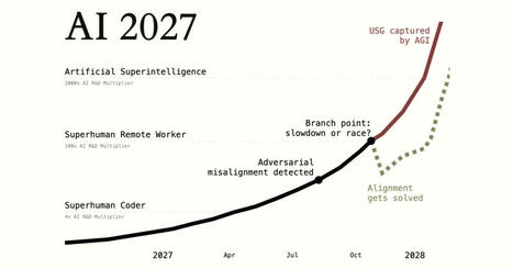
A research-backed AI scenario forecast for the next 2 years, thus an interesting look at how AI and AI agents may impact life within the next 2 years - 2027

Nik Peachey's curator insight,
April 16, 4:54 AM
An interesting look at how AI and AI agents may impact life within the next 2 years!!! https://ai-2027.com/

The installation of new CEO Lip-Bu Tan at chip stock Intel ($INTC) was supposed to be a turning point. But as it turns out, it is leaving behind a new
Richard Platt's insight:
The installation of new CEO Lip-Bu Tan at Intel was supposed to be a turning point. But as it turns out, it is leaving behind a new wake of uncertainty that is prompting concern. Apparently, Tan has a wide range of investments, many of which are in China…and some of which are even connected to the Chinese military. This was bad news as far as investors were concerned, and Intel shares plummeted over 7.5% in Thursday afternoon’s trading. Given that Tan put up $25 million of his own money to invest in Intel when he took the CEO slot, it should come as little surprise that he had substantial investments to begin with. Tan’s investments, reports noted, included “hundreds of Chinese tech firms.” The biggest surprise, though, was that at least 8 of these firms had direct ties to the People’s Liberation Army, the Chinese military. A review from Reuters found that Tan actually controls +40 Chinese companies outright. He has minority stakes in +600 beyond that as well. And this, investors believe, may “complicate” the notion of getting Intel back up and running. Andrew King with Bastille Ventures noted “The simple fact is that Mr. Tan is unqualified to serve as the head of any company competing against China, let alone one with actual intelligence and national security ramifications like Intel and its tremendous legacy connections to all areas of America’s intelligence and the defense ecosystem.”
|

AI chatbots are impersonating students to scam colleges for financial aid, also occupying online class spots, a recent report reveals.
Richard Platt's insight:
A concerning new trend is emerging in the world of cyber fraud. A recent report reveals how sophisticated AI chatbots are now impersonating students on a massive scale. Their goal is primarily to siphon off college financial aid and, alarmingly, even occupy coveted spots in online courses. This isn’t just theoretical; it’s a rapidly evolving scam that’s costing institutions millions. Plus, it is potentially displacing legitimate students right here in the US market and globally. These aren’t your run-of-the-mill spambots. These advanced chatbots leverage stolen personal data—often harvested from the countless data breaches we’ve seen—to create convincing student profiles. They boast compelling names, addresses, Social Security numbers, and academic histories. From this data, they apply for grants, loans, and college admissions, effectively masquerading as real individuals. The AP News report highlights that an increasing sophistication of AI is a major driver behind this emergence in fraudulent activity. The ability of these chatbots to convincingly mimic human applicants makes detection incredibly challenging for college admissions and financial aid offices. It particularly affects larger institutions and community colleges dealing with high application volumes. The financial losses for colleges are substantial, with some states already reporting millions in unrecoverable funds. Beyond the institutional impact, this also creates a significant risk of identity theft for the individuals whose stolen data is being used in these schemes.
Once they’re in, these “phantom students” might even engage minimally in online classes just long enough to get the desired financial aid. After that, they simply vanish. Disturbingly, there have been reports of entire online classrooms where there are only these AI imposters. This leaves genuine students struggling for access.

From
wccftech
Huawei hoped to wean off China from NVIDIA's dominance via its Ascend 910C GPUs, but continues to encounter substantial inertia.
Richard Platt's insight:
Huawei hoped to wean China off NVIDIA's dominant GPUs via Ascend 910C GPUs, but Huawei continues to encounter substantial resistance to this, courtesy of NVIDIA's ecosystem lock-ins via the CUDA software and Huawei's own shortcomings. It's now reported that China's tech titans, including TikTok's parent ByteDance, Alibaba, and Tencent, have yet to order Huawei's AI chips in large quantities. Several factors create a sizable inertia around Huawei's 910C GPUs: (1) Many of China's tech titans are invested in NVIDIA's CUDA ecosystem, and any break from NVIDIA will entail a significant investment of time and resources, many expect Huawei to adapt to their platforms instead of the other way around. (2) China's largest tech companies are competitors of Huawei and, feel reluctant to go all-in on their competitor's offering. (3) Huawei's Ascend 910C ICs suffer from periodic overheating issues, that affects the perception of reliability. (4) China's largest tech companies stashed away a sizable repository of NVIDIA's GPUs over the years, inventory has yet to run out (5) US Department of Commerce issued sweeping guidance that any company that using Huawei's ICs without prior authorization could be deemed to be in violation of US export controls.

From
www
South Korea's newly elected President Lee Jae-myung has unveiled a flagship policy offering up to 10% production tax credits for semiconductors manufactured and sold domestically, marking a shift from the country's traditional investment-based incentives to output-focused support similar to US measures under the Inflation Reduction Act.
Richard Platt's insight:
Shanghai-based UniVista Industrial Software Group recently announced it now offers Chinese users free access to Electronic Design Automation (EDA) software. UniVista called the announcement a “technological counterattack” indicating it is responding to blockades and restrictions imposed by the U.S.. Reuters reported that the Trump administration has told US-based companies to stop selling software used to design chips to Chinese customers. Leading companies like Cadence, Synopsys, and Siemens EDA were notified. The 3 companies account for 70% of China’s EDA market, it was reported that Synopsys has told its staff in China to halt sales and stop taking new orders. UniVista, founded in 2020, comprises multiple former Execs of Synopsys and Cadence, several of whom held Senior VP and Fellow-level positions. Besides UniVista, prominent players in China’s EDA ecosystem include Empyrean Technology, Primarius Technologies and Semitronix. As of 2024, Empyrean held 6% of China’s market, Chiana's largest EDA player. EDA tools are software for assisting engineers in designing, simulating, and verifying ICs, PCBs, and SoCs. EDA tools are considered essential for IC design processes. UniVista’s offers EDA tools, including a simulator debugger, a DFT platform, and a PCB design platform.

Officials uncover how North Korean operatives used stolen identities and remote-controlled tech to infiltrate American companies and steal corporate data.
Richard Platt's insight:
North Korean hackers operated a “laptop farm” scheme using fake identities to land remote US tech jobs and illegally collect $17.1 million in wages. Part of a broader effort to exploit global labor markets through cybercrime. Cybersecurity experts described the operation as “something we’d never seen before,” citing sophisticated tactics and custom-built programs enabling North Korean agents to bypass detection systems and exfiltrate sensitive corporate data. Federal court documents and a report from the WSJ, North Korean IT workers ran a covert operation where dozens of US-based laptops, remotely controlled using compromised identities, allowing them to pose as job seekers in the US tech sector, securing employment with US companies. Once hired, the “workers” funneled salaries, using proxy accounts and intermediaries. Several Americans unknowingly or willfully participated by setting up and maintaining laptop farms, receiving employer-issued hardware, and managing employment documents, giving North Korean operatives direct access to corporate systems. North Korea’s strategy of infiltrating remote jobs is not limited to the US; the UK and EU countries were as well. More aggressive tactics are being deployed in these regions, with the hackers threatening to leak proprietary information if their contracts are terminated. This evolving pattern highlights North Korea’s ability to adapt its cyber tactics across borders, turning the global remote work economy into a new frontier for illicit revenue and intelligence gathering.
From
www
Richard Platt's insight:
Arm highlights the arrival of Zena CSS as an stepping stone to accelerate the developing of AI-defined vehicles. From the broader automotive semiconductor landscape and the competitive landscape for automotive compute is dynamic, with established semiconductor companies offering various System-on-Chips (SoCs) and platforms. Players like NVIDIA, Qualcomm, Intel/Mobileye, Renesas, and NXP provide a range of solutions for high-performance ADAS/AD compute, digital cockpits, and vehicle control. These companies are developing increasingly complex and heterogeneous SoCs featuring powerful CPUs, GPUs, and specialized AI accelerators (NPUs) to handle the demands of the AI-defined vehicle. Within this landscape, the RISC-V open-standard instruction set architecture (ISA) is also emerging as a pivotal technology, particularly in the European and Asian automotive sectors. Infineon announced a new RISC-V-based AURIX microcontroller family and NXP is leveraging RISC-V for specialized accelerators. Arm’s approach with Zena CSS is distinct. As Ms. Vachani clarified, Arm is not building and marketing its own ultimate chips like these companies. Instead, Arm licenses its IP cores and now, with Zena CSS, offers a larger, pre-integrated subsystem. This allows Arm’s partners—including semiconductor companies, Tier 1 suppliers, and potentially others—to build their own differentiated SoCs more rapidly and with reduced risk.

A corporate breakup appears off the table, for now, but layoffs could start within weeks.
Richard Platt's insight:
Intel's Private Equity CEO Lip-Bu Tan is shaking up the company’s organizational structure and cutting costs but isn’t remaking its strategy. “I think it’s a fair assessment that Lip-Bu isn’t thinking about massive changes,” CFO David Zinsner told a J.P. Morgan conference in Boston. Intel spent months in limbo after its board forced out ex-CEO Pat Gelsinger in early December. Company executives openly discussed the possibility of breaking up the business, separating its chip design business from Intel’s manufacturing arm. Once the world’s largest chipmaker, Intel is trying to recover from an extended decline in sales and a $19 billion loss in 2024. A plan pushed by Gelsinger, and only later embraced by Tan, aims to open Intel’s factories to make chips for other companies. Since Intel hired Tan in March, he's emphasized taking steps to improve Intel’s decision-making and has said nothing about splitting the business. Instead, Tan has said he plans to reduce the layers of management and implement “several months” of job cuts to cut costs and flatten the organization. “When he looks at the business, what he feels is the biggest issue at this point is a lack of execution”. Intel hasn’t said how many jobs it will cut altogether. But telling factory workers last week that it is making layoff decisions this month and will notify staff by the middle of June. Tan said, “We must balance our reductions with the need to retain and recruit key talent. Removing layers of management will give engineers more voice in product design, and a closer connection with Intel customers. He also said fewer layers of management will provide Tan a clearer view of how the company is operating. “What he wants is the lowest level of the organization to be closer to him,” Intel has been slow to attract customers to its contract manufacturing business, (Intel Foundry). Intel doesn’t have significant commitments from potential clients yet for its new 18A manufacturing node. Intel still expects its factory business will break even in 2027, Zinsner saying it's “a little bit embarrassing” that Intel hasn’t been delivering better products to customers. Intel cut 15,000 jobs in 2024, and employees say privately that morale is low this spring with the prospect of additional layoffs to come. Some employees are also unhappy with Tan’s decision to order workers back to the office 4 days a week. Zinsner blamed remote work for some of the company’s issues. “We did have a number of the team that was not working on site full time,” “I think to some degree that has inhibited us and impacted our ability to execute on road maps and process.” Intel is now walking a narrow path, cutting costs, jobs and employee perks while trying to retain and recruit top technologists to improve its products. Zinsner said Tan is “a magnet for talent” stating it will become apparent soon that Intel is again a destination for top-level professionals in the semiconductor industry. “We have lost talent at the company, and we do need to rebuild that.”

According to CSIS, Huawei has millions of AI chips from SMIC despite yield problems.
Richard Platt's insight:
Huawei cannot legally obtain advanced chips made by TSMC, the company used shell companies last year to obtain compute chiplets for its Ascend 910 AI chips. The conspiracy was discovered by TechInsights and TSMC, which ceased to ship chiplets to Huawei's proxies and initiated an internal investigation. However, it was not clear how many chiplets it supplied to Huawei. According to a report by the Center for Strategic and International Studies, Huawei obtained as many as two million Ascend 910 AI chiplets. "However, TSMC manufactured large quantities of Huawei Ascend 910B chips on behalf of Huawei shell companies and shipped the chips to China in violation of U.S. export controls," the report by CSIS reads. According to the report, "government officials told CSIS that TSMC manufactured more than 2 million Ascend 910B logic dies and that all of these are now with Huawei. If true, this is enough dies to make 1 million Ascend 910C units. […] Even though Huawei likely has the more than 2 million Ascend 910B logic dies made by TSMC, there is a question as to whether it has enough HBM to integrate with those dies […] It seems likely that Huawei does, however, since the U.S. plan to restrict all advanced HBM sales to China on a country-wide basis was leaked to Bloomberg in August 2024 and did not go into effect until December of that year, giving Huawei ample time to legally acquire HBM chips as part of a stockpiling strategy." Although the report seems correct about Huawei's stockpiling strategy and even gives us an insight into how many chips TSMC produced for Huawei's intermediaries, it still contains several inaccuracies that lead to wrong conclusions. Huawei's original HiSilicon Ascend 910, which was launched in 2019, consists of a Virtuvian AI chiplet, a Nimbus V3 I/O die, four HBM2E memory stacks, and two dummy dies. TSMC produced Virtuvian chiplets for Huawei from 2019 to September 2020, using its N7+ process technology, a 7nm-class node with some EUV layers. After the U.S. government put Huawei on its Entity List in 2020, Huawei had to redesign its Virtuvian chiplet to make it at SMIC, which used its N+1 technology (1st Generation 7nm-class process) to build it. GPUs with the new Virtuvian chiplet are called HiSilicon Ascend 910B and have nothing to do with TSMC. Later, Huawei developed a more sophisticated version of its Virtuvian chiplet for its Ascend 910C, which SMIC makes using its 2nd Generation 7nm fabrication technology (N+2). Contrary to the report, the Ascend 910C has only one compute chiplet. Again, the Ascend 910C has nothing to do with TSMC. As Huawei managed to deceive TSMC, the latter produced the original Ascend 910 chiplet for the company in 2023 – 2024, as discovered by TechInsights. Another noteworthy thing about Huawei's Ascend 910B and Ascend 910C is that their yields are not exactly high, so most parts are shipped with some compute elements disabled. Also, only 75% of Huawei's AI chips survive advanced packaging, which is not a good result. "However, the advanced packaging process by which two Ascend 910B dies and HBM are combined into a unified Ascend 910C chip also introduces defects that can compromise the functionality of the chip," the report says. "Industry sources told CSIS that roughly 75% of the Ascend 910Cs currently survive the advanced packaging process." Nonetheless, Huawei continues to acquire millions of Ascend 910B and Ascend 910C for its internal AI projects and external customers. For example, DeepSeek claims that the Ascend 910C delivers 60% of the performance offered by Nvidia's H100, which may not be enough for training large language models but is good enough for inference workloads.

A former SK Hynix employee has been charged with stealing wafer bonding and image sensor technologies to secure a job at Huawei’s HiSilicon, raising alarm over tech IP leaks to China.
Richard Platt's insight:
A former SK Hynix employee has been formally accused of illegally transferring technologies related to advanced chip packaging used for 3D NAND, HBM, and multi-chiplet assemblies as well as CMOS image sensors to Huawei's HiSilicon division, reports DigiTimes citing the Seoul Central District Prosecutor's office. An interesting twist to this story: While working at Huawei, the suspect allegedly took IP related to CMOS image sensors (CIS) and hybrid bonding chip packaging technology that is used for 3D NAND, HBM3 / HBM3E / HBM4 memory, as well as Advanced Stacked multi-chiplet packages (e.g., TSMC's SoIC and Intel's Foveros 3D). Huawei did not explicitly ask the suspect to bring it SK hynix's trade secrets (even though the company is known for poaching highly-skilled employees from world-class companies by offering them huge salaries), but accepted them as part of the hiring process. It is unclear whether the suspect's targets were hybrid bonding and image sensors, or 'just' hybrid bonding as modern CMOS sensors also use hybrid bonding. SK Hynix reportedly clarified that the leaked bonding-related information concerned general wafer-to-wafer processes and not the specific hybrid bonding technique currently being developed or used for commercial products. For Chinese companies like Huawei (which does not have access to advanced process technologies and packaging methods used by TSMC and SK hynix) as well as SMIC (which does not have access to the latest lithography equipment made by ASML), getting wafer bonding know-how from SK hynix, which had licensed such technologies from Xperi, may be considered as a major breakthrough as wafer bonding is becoming increasingly important for multiple semiconductor applications. The individual in question, a South Korean citizen named only in the complaint by his surname, Kim, previously worked for the Chinese unit of SK hynix. Authorities allege that in 2022 he secured a position with HiSilicon and, during the hiring process, improperly accessed and misused internal data belonging to SK Hynix. Kim reportedly printed out and captured photographs of internal files against policy. Investigators discovered that over 11,000 photographs of confidential content were taken, and steps were allegedly made to mask the origin by removing company identifiers such as brand logos and secrecy labels from the images. Evidence indicates that Kim submitted these materials as part of job applications to two separate companies in China, using them to enhance his qualifications. Authorities now claim this was a calculated effort to secure employment using unlawfully obtained information from his former employer. The report confirms that many technologies developed in China in general and by Huawei specifically originate from multi-national corporations.

Word has reached SemiAccurate about the upcoming ARM branded server CPU.
Richard Platt's insight:
Word has reached SemiAccurate about the upcoming ARM branded server CPU. While the picture is not complete yet, we can now flesh out a lot of the details. SemiAccurate has long heard rumors of ARM making their own devices which on the surface appear to compete with some customers. The devices are real, they have customers, and the competition aspect is as unclear as it ever was. All this said, time to dive in.
Richard Platt's insight:
Sunlin Chou, who passed on December 5th, 2018, played his role and made contributions to the semiconductor industry in developing a new business model for semiconductor R&D. While his legacy had faded since he retired in 2005, his career included filling Gordon Moore’s shoes as a key technologist in the 2nd Gen of Semiconductor Technical Leadership. Sunlin Chou’s last position was running the Technology side of Intel’s Technology and Manufacturing Group. He was in that group of “Shadow Warriors” who ran R&D. They seldom get any public light, and only the people in their company know what they do. Yet they bear a tremendous burden. They must decide among the myriad of technologies, which ones deserve attention, funding, etc. They must ply the foggy seas of the tech triangle that lie between customer need, realization in product, and manufacturability. It is a place where shipwrecks occur all too often. For Sunlin, the challenge was even greater. He had to fill Gordon Moore’s shoes. That meant not only being right, but also being above industry politics. You can learn a lot from someone who has successfully sailed these seas. At the core of Sunlin’s values was the belief that all problems should be dealt with systematically. He was one of the most systematic individuals you would ever meet, exemplary in many ways: every hair was always in a precise place, clothing all in alignment, shoes polished, and a poker stare that came from years of making many calculated gambles on future technology. This is exactly how he dealt with the issue of reviving Intel’s prowess after the 1985 debacle. Sunlin’s role in this was to develop a new business model for R&D. While many people were looking for an outside solution, like consortia, Sunlin was looking inside to see how the process could be streamlined. Most knew the model wasn’t working well. R&D often never led anywhere for the companies that funded it (Xerox Parc being the best example). It was a money sink, because few innovations ever made it to the business side of an organization. Yet few did anything about it. -- Sunlin looked at these problems and saw the opportunity. -- Sunlin’s most important contribution is his R&D Pipeline model, where he applied the first systematic approach to the whole development cycle. Central to his method was a strong understanding of Moore’s Law and how it impacted product life cycles. It led to his decision to set technical direction based on its relentless progression. This led to node planning. What came next was truly innovative. First, he covered the horizontal time line with a flow model that started with the research infrastructure outside Intel; then feeding it inside to research; then to path finding, on to development; and finally, to manufacturing – all synchronized to the nodal clock. To do this, he had to create a Copy-Exactly infrastructure for R&D that had never existed. Plus, everything had to be tightly coupled at the hand-off points, which is where most fail. This was done with exacting business processes. Second, he also covered the vertical technology line, integrating the test, assembly, and process roadmaps into a single cohesive strategy/roadmap. It doesn’t get more systematic than this. The result was that Intel was able to shift into high gear, running on a 24-month nodal clock.
Richard Platt's insight:
Intel’s new CTO and AI Chief Sachin Katti is taking over responsibilities of Intel’s AI road map and strategy, the business unit most recently known as the Data Center and AI Group (DC&AI) will be split apart and “refocused” so that the Data Center part will focus on CPUs. These changes were detailed in memos sent last Thursday to Intel employees by Katti, and Karin Eibschitz, the interim GM of what is now being called the Data Center Group. Lip-Bu Tan also expanded the roles and responsibilities for Katti— already a part of Tan’s executive leadership team as the head of Intel’s Network and Edge Group (NEX). This will put him in charge of Intel’s “overall AI strategy and AI product road map as well as Intel Labs and our relationships with the startup and developer ecosystems,” Eibschitz’s division will continue to handle Data Center CPUs and Katti taking over Data Center accelerator chips such as GPUs in his newly configured AI and CTO organization. The Data Center Group will collaborate with new horizontal engineering teams—reporting directly to Tan and led by long-time technical leaders Rob Bruckner, Mike Hurley and Lisa Peace—as well as Katti’s new CTO and AI organization. In Tan’s memo to Intel employees, said he has asked each member of his executive team to “identify opportunities” for further organizational changes in support of his goals to reduce bureaucracy and speed up decision-making. “As I said last month, Intel is going to act like a disruptor again by giving engineers the freedom to innovate,”. “We will simplify the way we work so that it’s easier to get work done. And we will empower smaller, more focused teams to create great products and delight our customers,”. “Right now, we are implementing the highest-level [organization] changes while we continue to work through further refinements,” Eibschitz said of the Data Center Group.
|


Previous industry sources suggested that NVIDIA was exploring the use of Intel’s 18A process for its gaming GPUs, according to Tom’s Hardware. Now, interest in the 18A node appears to be growing. Chosun Biz notes that Microsoft has reportedly signed a large-scale foundry deal with Intel using the 18A process, while talks with Google are also said to be underway. It's been noted that a Microsoft deal would mark a major milestone for Intel boosting its standing against TSMC and Samsung in advanced foundry. - Intel’s 18A process is currently in risk production and is expected to enter high volume manufacturing (HVM) late 2025. Intel is developing two enhanced variants of its 18A node: 18A-P, slated for launch in 2026, and 18A-PT, expected in 2028, it was noted that initial 18A-P wafers have already been introduced in Intel’s fabs. Intel is working with lead customers on its next-gen 14A node and started sharing early 14A PDKs with key partners. Chosun Biz notes that Intel has the largest number of U.S.-based factories among foundry players, potentially offering it an advantage in mitigating tariff-related risks. Intel is currently building 2 cutting-edge fabs in Arizona, alongside an expansion of its advanced packaging facilities in New Mexico. In Oregon, Intel is also moving forward with a new 300mm logic and foundry plant. In Ohio, it has committed USD 28 billion to construct 2 additional factories; but operations are now expected to begin between 2030 and 2032.
Intel’s overseas expansion is picking up. in Ireland, HVM of the Intel 4 process is set to begin at Fab 34, with 3nm chip HVMN scheduled for later in 2025. In Israel, Fab 38 will produce HPC ICs using EUV lithography.