Your new post is loading...

|
Scooped by
Dr. Stefan Gruenwald
September 24, 2019 12:06 AM
|
A promising semiconductor material could be improved if flaws previously thought irrelevant to performance are reduced, according to research published today in Nature Communications. A group of researchers at Rensselaer Polytechnic Institute and other universities has shown that a specific defect impacts the ability of halide perovskite to hold energy derived from light in the form of electrons. “Defects could be good or bad in semiconductors,” said Jian Shi, associate professor of materials science engineering. “For some reason, people did not pay attention to dislocations in halide perovskite, but we have shown that this defect is a problem in halide perovskite.” Research on halide perovskite has rapidly improved the efficiency of the material from about a 3% conversion of light to electrical energy to 25% — equivalent to state-of-the-art silicon solar cells — over the course of a decade. Researchers wrestled with silicon for decades to reach that material’s current level of efficiency. Halide perovskite also has promising carrier dynamics, which are roughly defined as the length of time that light energy absorbed by the material is retained in the form of an excited electron. To make a good prospect for solar energy conversion, electrons in the material must retain their energy long enough to be harvested by an electrode attached to the material, thus completing the conversion of light to electrical energy. The material had long been considered “defect tolerant,” meaning flaws like missing atoms, shoddy bonds across grains of the crystal, and a mismatch known as crystallographic dislocation were not believed to have much impact on efficiency. More recent research has questioned that assumption and found that some defects do affect aspects of the crystal’s performance. Shi’s team tested whether the defect of crystallographic dislocation impacts carrier dynamics by growing the crystal on two different substrates. One substrate had a strong interaction with the halide perovskite as it was being deposited, producing a higher density of dislocations. The other had a weaker interaction and produced a lower density of dislocations. The results show that dislocations negatively impact the carrier dynamics of halide perovskite. Reducing dislocation densities by more than one order of magnitude is found to lead to an increase of electron lifetime by four times.
|
|
Scooped by
Dr. Stefan Gruenwald
September 9, 2019 10:10 PM
|
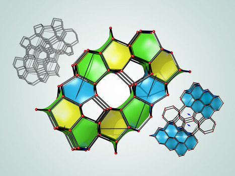
Superhard materials can slice, drill and polish other objects. They also hold potential for creating scratch-resistant coatings that could help keep expensive equipment safe from damage. Now, science is opening the door to the development of new materials with these seductive qualities. Researchers have used computational techniques to identify 43 previously unknown forms of carbon that are thought to be stable and superhard—including several predicted to be slightly harder than or nearly as hard as diamonds. Each new carbon variety consists of carbon atoms arranged in a distinct pattern in a crystal lattice. The study—published on Sept. 3, 2019, in the journal npj Computational Materials—combines computational predictions of crystal structures with machine learning to hunt for novel materials. The work is theoretical research, meaning that scientists have predicted the new carbon structures but have not created them yet. "Diamonds are right now the hardest material that is commercially available, but they are very expensive," says University at Buffalo chemist Eva Zurek. "I have colleagues who do high-pressure experiments in the lab, squeezing materials between diamonds, and they complain about how expensive it is when the diamonds break. "We would like to find something harder than a diamond. If you could find other materials that are hard, potentially you could make them cheaper. They might also have useful properties that diamonds don't have. Maybe they will interact differently with heat or electricity, for example."
|
|
Scooped by
Dr. Stefan Gruenwald
August 5, 2019 8:02 PM
|
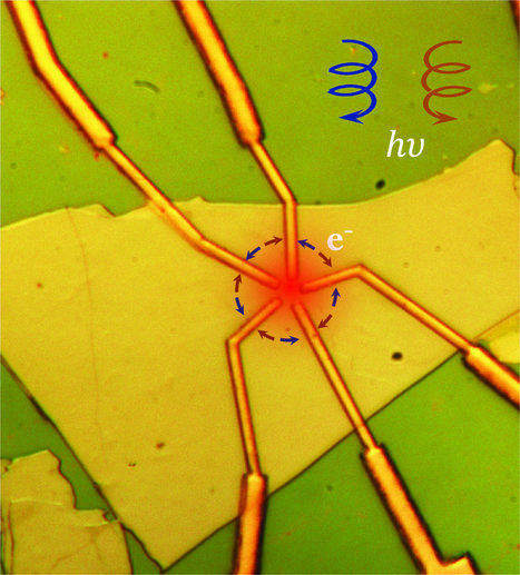
Insights from quantum physics have allowed engineers to incorporate components used in circuit boards, optical fibers, and control systems in new applications ranging from smartphones to advanced microprocessors. But, even with significant progress made in recent years, researchers are still looking for new and better ways to control the uniquely powerful electronic properties of quantum materials. A new study from Penn researchers found that Weyl semimetals, a class of quantum materials, have bulk quantum states whose electrical properties can be controlled using light. The project was led by Ritesh Agarwal and graduate student Zhurun Ji in the School of Engineering and Applied Science. The findings are published in Nature Materials. A hint of these unconventional photogalvanic properties, or the ability to generate electric current using light, was first reported by Agarwal in silicon. His group was able to control the movement of electrical current by changing the chirality, or the inherent symmetry of the arrangement of silicon atoms, on the surface of the material. "At that time, we were also trying to understand the properties of topological insulators, but we could not prove that what we were seeing was coming from those unique surface states," Agarwal explains. Then, while conducting new experiments on Weyl semimetals, where the unique quantum states exist in the bulk of the material, Agarwal and Ji got results that didn't match any theories that could explain how the electrical field was moving when activated by light. Instead of the electrical current flowing in a single direction, the current moved around the semimetal in a swirling circular pattern. Agarwal and Ji turned to Kane and Mele to help develop a new theoretical framework that could explain what they were seeing. After conducting new, extremely thorough experiments to iteratively eliminate all other possible explanations, the physicists were able to narrow the possible explanations to a single theory related to the structure of the light beam. "When you shine light on matter, it's natural to think about a beam of light as laterally uniform," says Mele. "What made these experiments work is that the beam has a boundary, and what made the current circulate had to do with its behavior at the edge of the beam." Using this new theoretical framework, and incorporating Rappe's insights on the electron energy levels inside the material, Ji was able to confirm the unique circular movements of the electrical current. The scientists also found that the current's direction could be controlled by changing the light beam's structure, such as changing the direction of its polarization or the frequency of the photons.
|
|
Scooped by
Dr. Stefan Gruenwald
July 16, 2019 3:47 PM
|
The ever-more-humble carbon nanotube may be just the device to make solar panels - and anything else that loses energy through heat - far more efficient. Rice University scientists are designing arrays of aligned single-wall carbon nanotubes to channel mid-infrared radiation (aka heat) and greatly raise the efficiency of solar energy systems. Gururaj Naik and Junichiro Kono of Rice's Brown School of Engineering introduced their technology in ACS Photonics. Their invention is a hyperbolic thermal emitter that can absorb intense heat that would otherwise be spewed into the atmosphere, squeeze it into a narrow bandwidth and emit it as light that can be turned into electricity. The discovery rests on another by Kono's group in 2016 when it found a simple method to make highly aligned, wafer-scale films of closely packed nanotubes. Discussions with Naik, who joined Rice in 2016, led the pair to see if the films could be used to direct "thermal photons." "Thermal photons are just photons emitted from a hot body," Kono said. "If you look at something hot with an infrared camera, you see it glow. The camera is capturing these thermally excited photons." Infrared radiation is a component of sunlight that delivers heat to the planet, but it's only a small part of the electromagnetic spectrum. "Any hot surface emits light as thermal radiation," Naik said. "The problem is that thermal radiation is broadband, while the conversion of light to electricity is efficient only if the emission is in a narrow band. "The challenge was to squeeze broadband photons into a narrow band," he said. The nanotube films presented an opportunity to isolate mid-infrared photons that would otherwise be wasted. "That's the motivation," Naik said. "A study by (co-lead author and Rice graduate student) Chloe Doiron found that about 20% of our industrial energy consumption is waste heat. That's about three years of electricity just for the state of Texas. That's a lot of energy being wasted.
|
|
Scooped by
Dr. Stefan Gruenwald
July 5, 2019 2:45 PM
|
In a paper released today in Science Advances, Australian researchers describe the first observation of a native ferroelectric metal: a native metal with bistable and electrically switchable spontaneous polarization states--the hallmark of ferroelectricity. The study found coexistence of native metallicity and ferroelectricity in bulk crystalline tungsten ditelluride (WTe2) at room temperature. A van-der-Waals material that is both metallic and ferroelectric in its bulk crystalline form at room temperature has potential for nano-electronics applications.
|
|
Scooped by
Dr. Stefan Gruenwald
June 13, 2019 9:18 PM
|
A new method of discovering materials using data analytics and electron microscopy has found a new class of extremely hard alloys. Such materials could potentially withstand severe impact from projectiles, thereby providing better protection of soldiers in combat. Researchers from Lehigh University describe the method and findings in an article, "Materials Informatics For the Screening of Multi-Principal Elements and High-Entropy Alloys," that appears today in Nature Communications. "We used materials informatics—the application of the methods of data science to materials problems—to predict a class of materials that have superior mechanical properties," said primary author Jeffrey M. Rickman, professor of materials science and engineering and physics and Class of '61 Professor at Lehigh University. Researchers also used experimental tools, such as electron microscopy, to gain insight into the physical mechanisms that led to the observed behavior in the class of materials known as high-entropy alloys (HEAs). High-entropy alloys contain many different elements that, when combined, may result in systems having beneficial and sometimes unexpected thermal and mechanical properties. For that reason, they are currently the subject of intense research. "We thought that the techniques that we have developed would be useful in identifying promising HEAs," Rickman said. "However, we found alloys that had hardness values that exceeded our initial expectations. Their hardness values are about a factor of 2 better than other, more typical high-entropy alloys and other relatively hard binary alloys."
|
|
Scooped by
Dr. Stefan Gruenwald
May 21, 2019 4:38 PM
|
Researchers discover surprising dielectric insulator for next-gen devices. Mixing two brittle materials to make something flexible defies common sense, but Rice University scientists have done just that to make a novel dielectric. Dielectrics are the polarized insulators in batteries and other devices that separate positive and negative electrodes. Without them, there are no electronic devices. The most common dielectrics contain brittle metal oxides and are less adaptable as devices shrink or get more flexible. So Rice scientists developed a dielectric poised to solve the problem for manufacturers who wish to create next-generation flexible electronics. Until now, manufacturers had to choose between brittle dielectrics with a high constant (K)—the material’s ability to be polarized by an electric field—or flexible low-K versions. The material created at Rice has both. Rice materials scientist Pulickel Ajayan and graduate student and lead author Sandhya Susarla combined sulfur and selenium to synthesize a dielectric that retains the best properties of high-K ceramics and polymers and low-K rubber and polyvinyl. “We were surprised by this discovery because neither sulfur or selenium have any dielectric properties or have a ductile nature,” Susarla said. “When we combined them, we started playing with the material and found out that mechanically, it behaved as a compliant polymer.” Their results appear in Science Advances.
|
|
Scooped by
Dr. Stefan Gruenwald
April 11, 2019 10:45 PM
|
Can water reach minus 263 degrees Celsius without turning into ice? Yes it can, say researchers from ETH Zurich and the University of Zurich, if it is confined in nanometre-scale lipid channels. Making ice cubes is a simple process: you take a plastic ice-cube tray like you'd find in most households, fill it with water and put it in the freezer. Before long, the water crystallizes and turns to ice. If you were to analyze the structure of ice crystals, you'd see that the water molecules are arranged in regular 3-dimensional lattice structures. In water, by contrast, the molecules are unorganized, which is the reason that water flows. Glassy water Led by Professors Raffaele Mezzenga and Ehud Landau, a group of physicists and chemists from ETH Zurich and the University of Zurich have now identified an unusual way to prevent water from forming ice crystals, so even at extreme sub-zero temperatures it retains the amorphous characteristics of a liquid. In a first step, the researchers designed and synthesized a new class of lipids (fat molecules) to create a new form of "soft" biological matter known as a lipidic mesophase. In this material, the lipids spontaneously self-assemble and aggregate to form membranes, behaving in a similar way as natural fat molecules. These membranes then adopt a uniform arrangement to form a network of connected channels that measure less than one nanometer in diameter. Temperature and water content, as well as the novel structure of the designed lipid molecules determine the structure that the lipidic mesophase takes. No space for water crystals What's so special about this structure is that -- unlike in an ice-cube tray -- there is no room in the narrow channels for water to form ice crystals, so it remains disordered even at extreme sub-zero temperatures. The lipids don't freeze either. Using liquid helium, the researchers were able to cool a lipidic mesophase consisting of a chemically modified monoacylglycerol to a temperature as low as minus 263 degrees Celsius, which is a mere 10 degrees above the absolute zero temperature, and still no ice crystals formed. At this temperature, the water became "glassy," as the researchers were able to demonstrate and confirm in a simulation. Their study of this unusual behaviour of water when confined within a lipidic mesophase was recently published in the journal Nature Nanotechnology. "The key factor is the ratio of lipids to water," explains Professor Raffaele Mezzenga from the Laboratory of Food & Soft Materials at ETH Zurich. Accordingly, it is the water content in the mixture that determines the temperatures at which the geometry of the mesophase changes. If, for example, the mixture contains 12 percent water by volume, the structure of the mesophase will transition at about minus 15 degrees Celsius from a cubic labyrinth to a lamellar structure. Natural antifreeze for bacteria "What makes developing these lipids so tricky is their synthesis and purification," says Ehud Landau, Professor of Chemistry at the University of Zurich. He explains that this is because lipid molecules have two parts; one that is hydrophobic (repels water) and one that is hydrophilic (attracts water). "This makes them extremely difficult to work with," he says. The soft biomaterial formed from the lipid membranes and water has a complex structure that minimizes the water's contact with the hydrophobic parts and maximizes its interface with the hydrophilic parts. The researchers modeled the new class of lipids on membranes of certain bacteria. These bacteria also produce a special class of self-assembling lipids that can naturally confine water in their interior, enabling the microorganisms to survive in very cold environments. "The novelty of our lipids is the introduction of highly strained three-membered rings into specific positions within the hydrophobic parts of the molecules," says Landau. "These enable the necessary curvature to produce such tiny water channels and prevent lipids to crystallize."
|
|
Scooped by
Dr. Stefan Gruenwald
March 20, 2019 8:26 PM
|
Electronics rule our world, but electrons rule our electronics. A research team at The Ohio State University has discovered a way to simplify how electronic devices use those electrons—using a material that can serve dual roles in electronics, where historically multiple materials have been necessary. The team published its findings today, March 18, in the journal Nature Materials. “We have essentially found a dual-personality material,” said Joseph Heremans, co-author of the study, professor of mechanical and aerospace engineering and Ohio Eminent Scholar in Nanotechnology at Ohio State. “It is a concept that did not exist before.” Their findings could mean a revamp of the way engineers create all different kinds of electronic devices. This includes everything from solar cells, to the light-emitting diodes in your television, to the transistors in your laptop, and to the light sensors in your smartphone camera. Those devices are the building blocks of electricity: Each electron has a negative charge and can radiate or absorb energy depending on how it is manipulated. Holes—essentially, the absence of an electron—have a positive charge. Electronic devices work by moving electrons and holes—essentially conducting electricity. But historically, each part of the electronic device could only act as electron-holder or a hole-holder, not both. That meant that electronics needed multiple layers—and multiple materials—to perform. But the Ohio State researchers found a material—NaSn2As2, a crystal that can be both electron-holder and hole-holder—potentially eliminating the need for multiple layers. “It is this dogma in science, that you have electrons or you have holes, but you don’t have both. But our findings flip that upside down,” said Wolfgang Windl, a professor of materials science and engineering at Ohio State, and co-author of the study. “And it’s not that an electron becomes a hole, because it’s the same assembly of particles. Here, if you look at the material one way, it looks like an electron, but if you look another way, it looks like a hole.” The finding could simplify our electronics, perhaps creating more efficient systems that operate more quickly and break down less often.
|
|
Scooped by
Dr. Stefan Gruenwald
March 14, 2019 12:58 AM
|
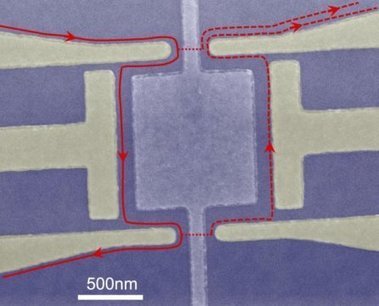
Researchers have created a new device that allows them to probe the interference of quasiparticles, potentially paving the way for the development of topological qubits. Qubits, the units used to encode information in quantum computing, are not all created equal. Some researchers believe that topological qubits, which are tougher and less susceptible to environmental noise than other kinds, may be the best medium for pushing quantum computing forward. Quantum physics deals with how fundamental particles interact and sometimes come together to form new particles called quasiparticles. Quasiparticles appear in fancy theoretical models, but observing and measuring them experimentally has been a challenge. With the creation of a new device that allows researchers to probe interference of quasiparticles, we may be one giant leap closer. The findings were published Monday in Nature Physics. "We're able to probe these particles by making them interfere," said Michael Manfra, the Bill and Dee O'Brian Chair Professor of Physics and Astronomy at Purdue University. "People have been trying to do this for a long time, but there have been major technical challenges." To study particles this small, Manfra's group builds teeny, tiny devices using a crystal growth technique that builds atomic layer by atomic layer, called molecular beam epitaxy. The devices are so small that they confine electrons to two dimensions. Like a marble rolling around on a tabletop, they can't move up or down. If the device, or "tabletop," is clean and smooth enough, what dominates the physics of the experiment is not electrons' individual actions, but how they interact with each other. To minimize the individual energy of particles, Manfra's team cooled them down to extremely low temperatures -- around -460 degrees Fahrenheit. Additionally, the electrons were subjected to a large magnetic field. Under these three conditions: extremely cold temperatures, confined to two dimensions, and exposed to a magnetic field, really strange physics starts to happen. Physicists call this the fractional quantum hall regime. "In these exotic conditions, electrons can arrange themselves so that the basic object looks like it carries one-third of an electron charge," said Manfra, who is also a professor of materials engineering, and electrical and computer engineering. "We think of elementary particles as either bosons or fermions, depending on the spin of the particle, but our quasiparticles have a much more complex behavior as they evolve around each other. Determining the charge and statistical properties of these states is a long-standing challenge in quantum physics." To make the particles interfere, Manfra's group built an interferometer: a device that merges two or more sources of quasiparticles to create an interference pattern. If you threw two stones into a pond, and their waves intersected at some point, this is where they would generate interference and the patterns would change. But replicating these effects on a much smaller scale is extremely difficult. In such a cramped space, electrons tend to repel each other, so it costs additional energy to fit another electron into the space. This tends to mess up the interference effects so researchers can't see them clearly. The Purdue interferometer overcomes this challenge by adding metallic plates only 25 nanometers away from the interfering quasiparticles. The metallic plates screen out the repulsive interactions, reducing energy cost and allowing interference to occur. The new device has identical walls on each side and metal gates, somewhat like a pinball machine. But unlike a pinball, which scatters around chaotically, the electrons in this device follow a very strict pattern. "The magic of the quantum hall effect is that all of the current will travel on the edge of the sample, not through the middle," said James Nakamura, Ph.D. candidate at Purdue and lead author of the paper. "When quasiparticles are tunneled across the beam splitter, they're split in half, in a quantum mechanical sense. That happens twice, at two beam splitters, and interference occurs between the two different paths." In such a bizarre realm of physics, it can be difficult for researchers to know if what they think they're seeing is what they're actually seeing. But these results show that, potentially for the first time, researchers have witnessed the quantum mechanical interference of quasiparticles.
|
|
Scooped by
Dr. Stefan Gruenwald
February 20, 2019 7:50 PM
|
Manipulation of paramagnetic microparticles can be exploited for drug delivery. Here the authors manipulate a swarm of such particles and control its shape with a magnetic field so that it can elongate reversibly, split into smaller swarms and thus be guided through a maze with multiple parallel channels. Mechanical engineers at the Chinese University of Hong Kong have created nanobots — tiny machines — that engage in swarming behavior, such as is found in bees, bacterial colonies and schools of fish. The researchers, who published their findings in Nature Communications, envision them used to deliver drugs in the body, treat blood clots or assist surgeons in performing complex tasks. “The nanobot swarm can be operated in a controlled fashion with a high speed, which has never been reported before,” said study leader Li Zhang. The researchers were inspired by the way animals swarm in nature: Ants, for instance, can use their bodies to build chains or bridges to get the colony across rough terrain. Zhang’s team used oscillating magnetic fields to influence the movement of the nanobots, which are each less than one micron wide, or a fifth of the size of a red blood cell; they found they could manipulate a bunch of tiny machines into elongating, splitting apart and merging back together.
|
|
Scooped by
Dr. Stefan Gruenwald
January 6, 2019 11:17 PM
|
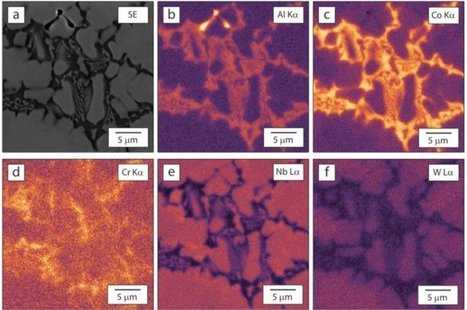
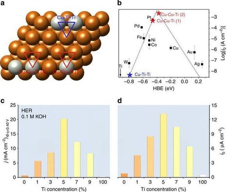
Investigations into non-precious metal catalysts for hydrogen evolution are ongoing. Here, the authors report that a hierarchical nanoporous copper-titanium bimetallic electrocatalyst is able to produce hydrogen from water under a mild overpotential at more than twice the rate of state-of-the-art carbon-supported platinum catalyst. Although both copper and titanium are known to be poor hydrogen evolution catalysts, the combination of these two elements creates unique copper-copper-titanium hollow sites, which have a hydrogen-binding energy very similar to that of platinum, resulting in an exceptional hydrogen evolution activity. In addition, the hierarchical porosity of the nanoporous copper-titanium catalyst also contributes to its high hydrogen evolution activity, because it provides a large-surface area for electrocatalytic hydrogen evolution, and improves the mass transport properties. Moreover, the catalyst is self-supported, eliminating the overpotential associated with the catalyst/support interface.
Researchers at Idaho National Laboratory have discovered how to make “superalloys” even more super, extending useful life by thousands of hours. The discovery could improve materials performance for electrical generators and nuclear reactors. The key is to heat and cool the superalloy in a specific way. That creates a microstructure within the material that can withstand high heat more than six times longer than an untreated counterpart.
“We came up with a way to make a superalloy that is much more resistant to heat-related failures. This could be useful in electricity generators and elsewhere,” said Subhashish Meher, an INL materials scientist. He was lead author of a new Science Advances paper describing the research. Alloys are combinations of two or more metallic elements. Superalloys are exceptionally strong and offer other significantly improved characteristics due to the addition of trace amounts of cobalt, ruthenium, rhenium or other elements to a base metal. Understanding how to build an improved superalloy is important for making the metallic mixture better for a particular purpose. Scientists have been studying nickel-based superalloys. Since these superalloys can withstand high heat and extreme mechanical forces, they are useful for electricity-generating turbines and high-temperature nuclear reactor components. Previous research had shown that performance can be improved if the material structure of the superalloy repeats in some way from very small sizes to very large, like a box within a box within a box. This is called a hierarchical microstructure. In a superalloy, it consists of a metallic matrix with precipitates, regions where the composition of the mixture differs from the rest of the metal. Embedded within the precipitates are still finer-scale particles that are the same composition as the matrix outside the precipitates – conceptually like nested boxes.
Via Alan Charky
|
|
|
Scooped by
Dr. Stefan Gruenwald
September 9, 2019 10:25 PM
|
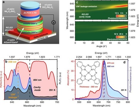
Polaritons are quasi-particles composed of a superposition of excitons and photons that can be created within a strongly coupled optical microcavity. Researchers now describe a structure in which a strongly coupled microcavity containing an organic semiconductor is coupled to a second microcavity containing a series of weakly coupled inorganic quantum wells. They were able to show that optical hybridization occurs between the optical modes of the two cavities, creating a delocalized polaritonic state. By electrically injecting electron–hole pairs into the inorganic quantum-well system, they were able to transfer energy between the cavities and populate organic-exciton polaritons. This approach represents a new strategy to create highly efficient devices for emerging ‘polaritonic’ technologies.
|
|
Scooped by
Dr. Stefan Gruenwald
August 30, 2019 1:54 PM
|
Spider webs are already strong enough to restrain small insects unlucky enough to fly into them, and soon, they may be capable of carrying the weight of a person. In a new study published in 2D Materials, Nicola Pugno at the University of Trento in Italy and his team detail how they cranked arachnids’ already impressive metabolic process up to 11 by adding graphene and carbon nanotubes to a spider’s drinking water. Afterward, the spider produced silk as it normally would, but the silk was five times stronger, putting it on par with the likes of pure carbon fibers and Kevlar — the strongest materials on Earth. “We already know that there are biominerals present in the protein matrices and hard tissues of insects, which gives them high strength and hardness in their jaws, mandibles, and teeth, for example,” Pugno told The Sydney Morning Herald. “So our study looked at whether spider silk’s properties could be ‘enhanced’ by artificially incorporating various different nanomaterials into the silk’s biological protein structures.” The enhanced webbing is still in the early phases of research, and Pugno’s results were derived from just a small amount of spider silk, so far more testing is required. If all goes as hoped, the research could eventually lead to millions of enhanced spiders producing webbing that can be used to make parachutes, rope, cables, and more.
|
|
Scooped by
Dr. Stefan Gruenwald
July 19, 2019 11:43 AM
|
Has your steering wheel been too hot to touch this summer? A new thermoelectric material reported in the journal Science could offer relief. The widespread adoption of thermoelectric devices that can directly convert electricity into thermal energy for cooling and heating has been hindered, in part, by the lack of materials that are both inexpensive and highly efficient at room temperature. Now researchers from the University of Houston and the Massachusetts Institute of Technology have reported the discovery of a new material that works efficiently at room temperature while requiring almost no costly tellurium, a major component of the current state-of-the-art material. The work, described in a paper published online by Science Thursday, July 18, has potential applications for keeping electronic devices, vehicles and other components from overheating, said Zhifeng Ren, corresponding author on the work and director of the Texas Center for Superconductivity at UH, where he is also M.D. Anderson Professor of Physics. “We have produced a new material, which is inexpensive but still performs almost as well as the traditional, more expensive material,” Ren said. The researchers say future work could close the slight performance gap between their new material and the traditional material, a bismuth-tellurium based alloy.
|
|
Scooped by
Dr. Stefan Gruenwald
July 11, 2019 12:19 PM
|
When the tension rises, unexpected things can happen – not least when it comes to gold atoms. Researchers from, among others, Chalmers University of Technology, have now managed, for the first time, to make the surface of a gold object melt at room temperature. Ludvig de Knoop, from Chalmers’ Department of Physics, placed a small piece of gold in an electron microscope. Observing it at the highest level of magnification and increasing the electric field step-by-step to extremely high levels, he was interested to see how it influenced the gold atoms. It was when he studied the atoms in the recordings from the microscope, that he saw something exciting. The surface layers of gold had actually melted – at room temperature. "I was really stunned by the discovery. This is an extraordinary phenomenon, and it gives us new, foundational knowledge of gold,” says Ludvig de Knoop. What happened was that the gold atoms became excited. Under the influence of the electric field, they suddenly lost their ordered structure and released almost all their connections to each other. Upon further experimentation, the researchers discovered that it was also possible to switch between a solid and a molten structure. The discovery of how gold atoms can lose their structure in this way is not just spectacular, but also groundbreaking scientifically. Together with the theoretician Mikael Juhani Kuisma, from the University of Jyväskylä in Finland, Ludvig de Knoop and colleagues have opened up new avenues in materials science. The results are now published in the journal Physical Review Materials.
|
|
Scooped by
Dr. Stefan Gruenwald
June 24, 2019 1:29 PM
|
By stretching like a rubber band to more than 25 times its original length, a new nanogenerator has set a new stretchability record. The triboelectric nanogenerator's 2500% stretchability represents a significant increase over the previous best values of approximately 1000%. In addition, the device is the first triboelectric nanogenerator that is completely fabricated with 3D printing. The researchers, including Kaushik Parida, Gurunathan Thangavel, and Pooi See Lee at Nanyang Technology University and the Singapore-HUJ Alliance for Research and Enterprise (SHARE), have published their results on the highly stretchable, all-3D-printed triboelectric nanogenerator in a recent issue of Nature Communications. Triboelectric nanogenerators (TENGs) harvest energy from ambient mechanical movements, such as finger tapping, and have potential applications as wearable electronic devices. Making TENGs stretchable is difficult because the two main layers—the triboelectric layer and the conductor—usually have different elastic properties, so they tend to come apart after repeated stretching. To address this issue, in the new study the researchers used the same elastic material (polyurethane acrylate, or PUA) as the basis for both the triboelectric layer and the polymer matrix for the conductor. To increase the conductivity, the researchers also added liquid metal particles and silver flakes to the conductor. When the nanogenerator undergoes extreme stretching, the hydrogen bonds in the PUA reversibly break and reform to support the desired stretchability. At the same time, the liquid metal particle shells break and release conductive liquid metal to provide a connection between the separated silver flakes in the PUA matrix, allowing the device to maintain a high conductivity. The researchers also demonstrated that the nanogenerator can be cut apart into separate pieces, and yet still almost completely regain its original performance after a healing process consisting of 24 hours of heating. The nanogenerator is also the first in which all components were printed using a 3D printer. Previously, only the triboelectric layer has been 3D-printed, since most elastomeric materials have limited stretchability when fabricated with 3D printing.
|
|
Scooped by
Dr. Stefan Gruenwald
May 21, 2019 4:47 PM
|
Scientists create an extraordinary, alien form of super hot ice. Researchers at Lawrence Livermore National Laboratory in California have created an extremely bizarre form of "superionic ice" which they have also dubbed as "ice XVIII". Researchers at Lawrence Livermore National Laboratory in California have created an extremely bizarre form of "superionic ice" which they have also dubbed as "ice XVIII". Its properties are quite extraordinary, one can even say that it is out of this world, something you'd only see in a sci-fi novel. The term "ice XVIII" came from a science fiction classic called Cats Cradle which was written by American writer Kurt Vonnegut. The climax of the story is where all of the world's ocean freezes over when it came into contact with a bizarre form of water, invented by one of the characters, known as "ice-nine" which is solid at room temperature. The "superionic ice" that researchers recently invented though doesn't freeze bodies of water that it comes into contact with, still, it is extremely extraordinary since it only exists at incredibly hot temperatures (around 5,000 degrees Fahrenheit) and extreme pressures 4 million times greater than Earth's atmospheric pressure. The creation of the "superionic ice" itself is done by using half a dozen giant laser beams to create shockwaves of increasing intensity that could flash-freeze tiny amounts of water. "We designed the experiments to compress the water so that it would freeze into solid ice, but it was not certain that the ice crystals would actually form and grow in the few billionths of a second that we can hold the pressure-temperature conditions," said Marius Millot, co-lead author on the paper. The science behind the experiment is complicated and it is explained in detail in Nature journal. Initially, the team demonstrated this form of ice via computer simulation. "Computer simulations have proposed a number of different possible crystalline structures for superionic ice. Our study provides a critical test to numerical methods." But this is the very first time they have actually created and imaged it on Earth.
|
|
Scooped by
Dr. Stefan Gruenwald
May 15, 2019 1:08 AM
|
Recently, there was an exciting discovery in the Graphene field of research. It was found that if you take two layers of graphene, and rotate one of the layers by a “magic angle” of 1.1°, then you can create a superconductor. A superconductor is a kind of material that conducts electricity with zero resistance. That means you could transport electrical power without any energy loss. Or you could create so much electrical current that it creates a powerful magnet (used in MRI machines). Superconductors also have special magnetic properties that allow for magnetic levitation (used in maglev trains). But superconductors need to be cooled below a certain temperature to work, otherwise they’re just ordinary materials. So, why would you ever try rotating two layers of graphene? Graphene is simply a layer of carbon atoms that form a hexagonal pattern. If you overlay two hexagonal patterns with a bit of rotation, you create what’s called a Moiré pattern. Basically, in some regions, the two layers of graphene are aligned, and in other regions, they are misaligned. In the image above, the regions of alignment appear “brighter” than the regions of misalignment (try squinting if you can’t see it). The regions of alignment and misalignment alternate in a repeating pattern. The repeating pattern of alignment and misalignment form a hexagonal grid. That grid is called the superlattice. The researchers who discovered this say that there’s an entire series of magic angles, and 1.1° is only the first one. I thought they meant that 1.1° is the smallest angle, but actually it’s the largest! The next few magic angles are 0.5°, 0.35°, 0.24°, and 0.2°. Apparently these angles are very precise. Physicists have predicted that something strange would happen at these angles for years, and it took an experimentalist to build a device that could control the angles precisely enough. Rotating the graphene by the magic angle is not, by itself, sufficient to create a superconductor. Magic angle graphene is a kind of material called a mott insulator, which actually conducts electricity very poorly. However, the most famous kind of unconventional superconductors, the cuprates, are created by “doping” mott insulators (which means introducing impurities). So the researchers tried doping magic angle graphene, and they found a superconductor. The superconductor only works at a temperature of 1.7 degrees above absolute zero, which isn’t much, but the similarity to cuprates means it could be a useful tool to understand what’s really going on.
|
|
Scooped by
Dr. Stefan Gruenwald
March 22, 2019 11:34 PM
|
Engineering professor Nader Engheta and his team have demonstrated a metamaterial device that can function as an analog computer, validating an earlier theory. For Nader Engheta of the School of Engineering and Applied Science, one of the loftier goals in this field has been to design metamaterials that can solve equations. This “photonic calculus” would work by encoding parameters into the properties of an incoming electromagnetic wave and sending it through a metamaterial device; once inside, the device’s unique structure would manipulate the wave in such a way that it would exit encoded with the solution to a pre-set integral equation for that arbitrary input. In a paper published in Science, Engheta and his team demonstrated such a device for the first time. Their proof-of-concept experiment was conducted with microwaves, as the long wavelengths allowed for an easier-to-construct macro-scale device. The principles behind their findings, however, can be scaled down to light waves, eventually fitting onto a microchip. Such metamaterial devices would function as analog computers that operate with light, rather than electricity. They could solve integral equations—ubiquitous problems in every branch of science and engineering—orders of magnitude faster than their digital counterparts, while using less power. Engheta, the H. Nedwill Ramsey Professor in the Department of Electrical and Systems Engineering, conducted the study along with lab members Nasim Mohammadi Estakhri and Brian Edwards. This approach has its roots in analog computing. The first analog computers solved mathematical problems using physical elements, such as slide-rules and sets of gears, that were manipulated in precise ways to arrive at a solution. In the mid-20th century, electronic analog computers replaced the mechanical ones, with series of resistors, capacitors, inductors, and amplifiers replacing their predecessors’ clockworks. Such computers were state-of-the-art, as they could solve large tables of information all at once, but were limited to the class of problems they were pre-designed to handle. The advent of reconfigurable, programmable digital computers, starting with ENIAC, constructed at Penn in 1945, made them obsolete. As the field of metamaterials developed, Engheta and his team devised a way of bringing the concepts behind analog computing into the 21stcentury. Publishing a theoretical outline for “photonic calculus” in Science in 2014, they showed how a carefully designed metamaterial could perform mathematical operations on the profile of a wave passing thought it, such as finding its first or second derivative.
|
|
Scooped by
Dr. Stefan Gruenwald
March 20, 2019 4:54 PM
|
Boston University researchers, Xin Zhang, a professor at the College of Engineering, and Reza Ghaffarivardavagh, a Ph.D. student in the Department of Mechanical Engineering, released a paper in Physical Review B demonstrating it's possible to silence noise using an open, ringlike structure, created to mathematically perfect specifications, for cutting out sounds while maintaining airflow. "Today's sound barriers are literally thick heavy walls," says Ghaffarivardavagh. Although noise-mitigating barricades, called sound baffles, can help drown out the whoosh of rush hour traffic or contain the symphony of music within concert hall walls, they are a clunky approach not well suited to situations where airflow is also critical. Imagine barricading a jet engine's exhaust vent -- the plane would never leave the ground. Instead, workers on the tarmac wear earplugs to protect their hearing from the deafening roar. Ghaffarivardavagh and Zhang let mathematics -- a shared passion that has buoyed both of their engineering careers and made them well-suited research partners -- guide them toward a workable design for what the acoustic metamaterial would look like. They calculated the dimensions and specifications that the metamaterial would need to have in order to interfere with the transmitted sound waves, preventing sound -- but not air -- from being radiated through the open structure. The basic premise is that the metamaterial needs to be shaped in such a way that it sends incoming sounds back to where they came from, they say. As a test case, they decided to create a structure that could silence sound from a loudspeaker. Based on their calculations, they modeled the physical dimensions that would most effectively silence noises. Bringing those models to life, they used 3D printing to materialize an open, noise-canceling structure made of plastic. Trying it out in the lab, the researchers sealed the loudspeaker into one end of a PVC pipe. On the other end, the tailor-made acoustic metamaterial was fastened into the opening. With the hit of the play button, the experimental loudspeaker set-up came oh-so-quietly to life in the lab. Standing in the room, based on your sense of hearing alone, you'd never know that the loudspeaker was blasting an irritatingly high-pitched note. If, however, you peered into the PVC pipe, you would see the loudspeaker's subwoofers thrumming away. The metamaterial, ringing around the internal perimeter of the pipe's mouth, worked like a mute button incarnate until the moment when Ghaffarivardavagh reached down and pulled it free. The lab suddenly echoed with the screeching of the loudspeaker's tune. "The moment we first placed and removed the silencer...was literally night and day," says Jacob Nikolajczyk, who in addition to being a study co author and former undergraduate researcher in Zhang's lab is a passionate vocal performer. "We had been seeing these sorts of results in our computer modeling for months -- but it is one thing to see modeled sound pressure levels on a computer, and another to hear its impact yourself."
|
|
Scooped by
Dr. Stefan Gruenwald
March 11, 2019 11:52 PM
|
A team of researchers led by the Department of Energy’s Lawrence Berkeley National Laboratory (Berkeley Lab) has developed a simple method that could turn ordinary semiconducting materials into quantum machines – superthin devices marked by extraordinary electronic behavior. Such an advancement could help to revolutionize a number of industries aiming for energy-efficient electronic systems – and provide a platform for exotic new physics. The study describing the method, which stacks together 2D layers of tungsten disulfide and tungsten diselenide to create an intricately patterned material, or superlattice, was published online recently in the journal Nature. “This is an amazing discovery because we didn’t think of these semiconducting materials as strongly interacting,” said Feng Wang, a condensed matter physicist with Berkeley Lab’s Materials Sciences Division and professor of physics at UC Berkeley. “Now this work has brought these seemingly ordinary semiconductors into the quantum materials space.” Two-dimensional (2D) materials, which are just one atom thick, are like nanosized building blocks that can be stacked arbitrarily to form tiny devices. When the lattices of two 2D materials are similar and well-aligned, a repeating pattern called a moiré superlattice can form. For the past decade, researchers have been studying ways to combine different 2D materials, often starting with graphene – a material known for its ability to efficiently conduct heat and electricity. Out of this body of work, other researchers had discovered that moiré superlattices formed with graphene exhibit exotic physics such as superconductivity when the layers are aligned at just the right angle. The new study, led by Wang, used 2D samples of semiconducting materials – tungsten disulfide and tungsten diselenide – to show that the twist angle between layers provides a “tuning knob” to turn a 2D semiconducting system into an exotic quantum material with highly interacting electrons.
|
|
Scooped by
Dr. Stefan Gruenwald
January 23, 2019 10:45 AM
|
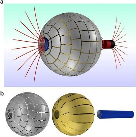
Wormholes are fascinating cosmological objects that can connect two distant regions of the universe. Because of their intriguing nature, constructing a wormhole in a lab seems a formidable task. A theoretical proposal by Greenleaf et al. presented a strategy to build a wormhole for electromagnetic waves. Based on metamaterials, it could allow electromagnetic wave propagation between two points in space through an invisible tunnel. However, an actual realization has not been possible until now. Scientists have now indeed succeeded to construct and experimentally demonstrate a magnetostatic wormhole. Using magnetic metamaterials and metasurfaces, their wormhole transfers the magnetic field from one point in space to another through a path that is magnetically undetectable. They experimentally show that the magnetic field from a source at one end of the wormhole appears at the other end as an isolated magnetic monopolar field, creating the illusion of a magnetic field propagating through a tunnel outside the 3D space. Practical applications of the results can be envisaged, including medical techniques based on magnetism.
|
|
Scooped by
Dr. Stefan Gruenwald
January 2, 2019 10:54 AM
|
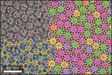
Brown University researchers have discovered a new type of quasicrystal, a class of materials whose existence was thought to be impossible until the 1980s. The strange class of materials known as quasicrystals has a new member. In a paper published on Thursday, Dec. 20, in Science, researchers from Brown University describe a quasicrystalline superlattice that self-assembles from a single type of nanoparticle building blocks. This is the first definitive observation of a quasicrystalline superlattice formed from a single component, the researchers say. The discovery provides new insight into how these strange crystal-like structures can emerge. “Single-component quasicrystal lattices have been predicted mathematically and in computer simulations, but hadn’t been demonstrated before this,” said Ou Chen, an assistant professor of chemistry at Brown and the paper’s senior author. “It’s a fundamentally new type of quasicrystal, and we’ve been able to figure out the rules for making it, which will be useful in the continued study of quasicrystal structures.” Quasicrystal materials were first discovered in the 1980s by the chemist Dan Shechtman, who in 2011 was awarded the Nobel Prize for the discovery. Unlike crystals, which consist of ordered patterns that repeat, quasicrystals are ordered but their patterns don’t repeat. Quasicrystals also have symmetries that aren’t possible in traditional crystals. Normal crystals, for example, can have three-fold symmetries that emerge from repeating triangles or four-fold symmetry from repeating cubes. Two- and six-fold symmetries are also possible. But quasicrystals can have exotic five-, 10- or 12-fold symmetries, all of which are “forbidden” in normal crystals. The first quasicrystalline materials discovered were metal alloys, usually aluminum with one or more other metals. So far, these materials have found use as non-stick coatings for frying pans and anti-corrosive coatings for surgical equipment. But there’s been much interest in making new types of quasicrystal materials — including materials made from self-assembling nanoparticles.
|