 Your new post is loading...
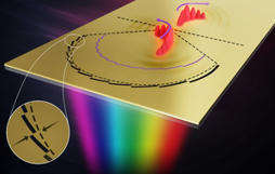
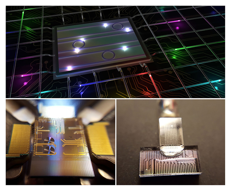
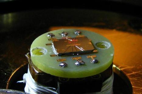
A new technique greatly reduces the error in an optical neural network, which uses light to process data instead of electrical signals. With their technique, the larger an optical neural network becomes, the lower the error in its computations. This could enable them to scale these devices up so they would be large enough for commercial uses. As machine-learning models become larger and more complex, they require faster and more energy-efficient hardware to perform computations. Conventional digital computers are struggling to keep up. An analog optical neural network could perform the same tasks as a digital one, such as image classification or speech recognition, but because computations are performed using light instead of electrical signals, optical neural networks can run many times faster while consuming less energy. However, these analog devices are prone to hardware errors that can make computations less precise. Microscopic imperfections in hardware components are one cause of these errors. In an optical neural network that has many connected components, errors can quickly accumulate. Even with error-correction techniques, due to fundamental properties of the devices that make up an optical neural network, some amount of error is unavoidable. A network that is large enough to be implemented in the real world would be far too imprecise to be effective. MIT researchers have overcome this hurdle and found a way to effectively scale an optical neural network. By adding a tiny hardware component to the optical switches that form the network’s architecture, they can reduce even the uncorrectable errors that would otherwise accumulate in the device. Their work could enable a super-fast, energy-efficient, analog neural network that can function with the same accuracy as a digital one. With this technique, as an optical circuit becomes larger, the amount of error in its computations actually decreases. “This is remarkable, as it runs counter to the intuition of analog systems, where larger circuits are supposed to have higher errors, so that errors set a limit on scalability. This present paper allows us to address the scalability question of these systems with an unambiguous ‘yes,’” says lead author Ryan Hamerly, a visiting scientist in the MIT Research Laboratory for Electronics (RLE) and Quantum Photonics Laboratory and senior scientist at NTT Research. Hamerly’s co-authors are graduate student Saumil Bandyopadhyay and senior author Dirk Englund, an associate professor in the MIT Department of Electrical Engineering and Computer Science (EECS), leader of the Quantum Photonics Laboratory, and member of the RLE. The research is published today in Nature Communications.
A new publication from Opto-Electronic Advances; DOI 10.29026/oea.2022.210047 discusses spatiotemporal manipulation of femtosecond light pulses for on-chip devices. With the development of highly integrated nanophotonic devices, researchers have begun to pursue new methods of flexibly manipulating the on-chip light signals in both extremely small spatial scale (e.g. nanometre) and ultrafast temporal scale (e.g. femtosecond). The control of optical signals in nanometre and femtosecond scales not only provides fundamental insights into the ultrafast dynamics of the interaction between light and matter, but also offers an effective platform for high-efficiency ultrafast signal processing in integrated nanophotonic devices, and optical detection and imaging with super-spatiotemporal resolution. Thus, research of spatiotemporal light-field manipulation is of great significance and can be widely applied in the fields of photonic circuits, photonic information processing, quantum information processing, neuromorphic computing and artificial intelligence, and ultrafast optical wavefront measurement. For the spatial modulation of light in nanoscale, in recent years some new optical devices such as metamaterials and metasurfaces have been rapidly developed to precisely control the behavior of micro- and nano-scale optical field. For example, the propagation of optical signals can be modulated to a curved trajectory as the Airy beam. For the modulation in time domain, the traditional methods, including dynamically controlled equipment (such as SLM) or actively controlled materials (such as electro-optical materials), suffer from the limited response time of materials and are not suitable for ultrafast modulation of femtosecond light pulses. Recently, with the development of pulse shaping technology, frequency-domain modulation has gradually become the main means of ultrafast modulation on femtosecond pulses. By combining the frequency-domain modulation method with the designed micro-/nano-structures, it is expected to achieve the light-field generation and manipulation in both nanometre and femtosecond scales, creating many novel spatiotemporal light fields and expanding new applications. The authors of this article propose a novel method to manipulate the on-chip propagation of a femtosecond light pulse based on the spatiotemporal Fourier transform (FT). By combining the frequency-domain modulation method with the spatial modulation method, they found that the spatial distribution of the light field can be arranged by regulating the spatial domain FT with an on-chip nanofocusing structure, and the ultrafast wavefront shaping of femtosecond pulses in the time domain can be realized by adjusting the temporal FT with the dispersion effect of light. Finally, the spatiotemporal FT can be synchronized to manipulate the on-chip propagation properties of femtosecond pulses in time-space domain.
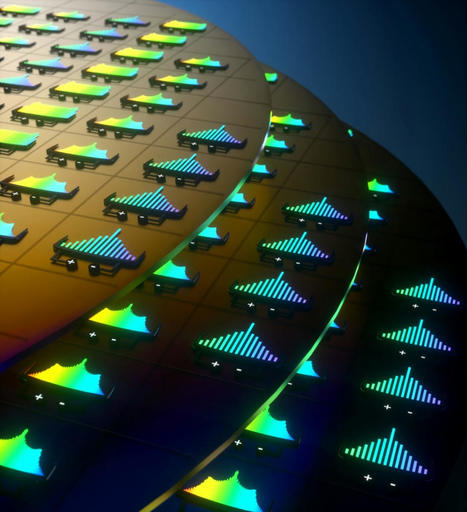
Fifteen years ago, UC Santa Barbara electrical and materials professor John Bowers pioneered a method for integrating a laser onto a silicon wafer. The technology has since been widely deployed in combination with other silicon photonics devices to replace the copper-wire interconnects that formerly linked servers at data centers, dramatically increasing energy efficiency -- an important endeavor at a time when data traffic is growing by roughly 25% per year. For several years, the Bowers group has collaborated with the group of Tobias J. Kippenberg at the Swiss Federal Institute of Technology (EPFL), within the Defense Advanced Research Projects Agency (DARPA) Direct On-Chip Digital Optical Synthesizer (DODOS) program. The Kippenberg group discovered "microcombs," a series of parallel, low-noise, highly stable laser lines. Each of the many lines of the laser comb can carry information, extensively multiplying the amount of data that can be sent by a single laser. Recently, several teams demonstrated very compact combs by placing a semiconductor laser chip and a separate silicon nitride ring-resonator chip very close together. However, the laser and the resonator were still separate devices, made independently and then placed in close proximity to each other perfectly aligned, a costly and time-consuming process that is not scalable. The Bowers lab has worked with the Kippenberg lab to develop an integrated on-chip semiconductor laser and resonator capable of producing a laser microcomb. A paper titled "Laser soliton microcombs heterogeneously integrated on silicon," published in the new issue of the journal Science, describes the labs' success in becoming the first to achieve that goal. Soliton microcombs are optical frequency combs that emit mutually coherent laser lines -- that is, lines that are in constant, unchanging phase relative to each other. The technology is applied in the areas of optical timing, metrology and sensing. Recent field demonstrations include multi-terabit-per-second optical communications, ultrafast light detection and ranging (LiDAR), neuromorphic computing, and astrophysical spectrometer calibration for planet searching, to name several. It is a powerful tool that normally requires exceptionally high power and expensive lasers and sophisticated optical coupling to function. The working principle of a laser microcomb, explained lead author Chao Xiang, a postdoctoral researcher and newly minted Ph.D. in Bowers's lab, is that a distributed feedback (DFB) laser produces one laser line. That line then passes through an optical phase controller and enters the micro-ring resonator, causing the power intensity to increase as the light travels around the ring. If the intensity reaches a certain threshold, non-linear optical effects occur, causing the one laser line to create two additional, identical lines on either side. Each of those two "side lines" creates others, leading to a cascade of laser-line generation. "You end up with a series of mutually coherent frequency combs," Xiang said -- and a vastly expanded ability to transmit data. This research enables semiconductor lasers to be seamlessly integrated with low-loss nonlinear optical micro-resonators -- "low-loss" because the light can travel in the waveguide without losing a significant amount of its intensity over distance. No optical coupling is required, and the device is entirely electrically controlled. Importantly, the new technology lends itself to commercial-scale production, because thousands of devices can be made from a single wafer using industry standard complementary metal oxide semiconductor (CMOS)-compatible techniques. "Our approach paves the way for large-volume, low-cost manufacturing of chip-based frequency combs for next-generation high-capacity transceivers, data centers, space and mobile platforms," the researchers stated.
Quantum technologies such as quantum computers require sources of entangled pairs of photons. To make these photon pairs, researchers commonly use silicon-based devices, where the silicon sits on an insulator. Galan Moody and his colleagues at the University of California, Santa Barbara, wondered if they could switch the silicon with aluminum gallium arsenide (AlGaAs), a material that has recently been demonstrated to be useful for classical photonics applications. The team showed that AlGaAs-made devices can produce entangled photons at a rate 1000 times greater than devices made from other materials [1]. Chip-sized devices for producing entangled pairs of photons typically couple laser light into a photonic waveguide or an optical cavity. Individual photons in the laser are then annihilated by interacting with the cavity’s material, a process that creates two new—entangled—photons. The efficiency of this process depends on the size of the cavity and the properties of the material used to make it. Using this same design, Moody and his colleagues tinkered with the cavity’s size and switched its material from silicon to AlGaAs. They found that they could increase the efficiency of the process significantly without compromising other important properties of the generated entangled photon pairs, such as entanglement fidelity. The 1000-fold increase in brightness that the team achieved should, they say, let them produce the same number of entangled photon pairs as other devices but by using lower-power lasers. That could allow the modified devices to consume less power overall. AlGaAs could also be used to make the other components for quantum computers, potentially allowing them to be contained on a single chip. The team says that such integration would simplify device fabrication and facilitate all-on-chip quantum-photonics systems.
Researchers from the Harvard John A. Paulson School of Engineering and Applied Sciences (SEAS), in collaboration with researchers at McMaster University and University of Pittsburgh, have developed a new platform for all-optical computing, meaning computations done solely with beams of light. "Most computation right now uses hard materials such as metal wires, semiconductors and photodiodes to couple electronics to light," said Amos Meeks, a graduate student at SEAS and co-first author of the research. "The idea behind all-optical computing is to remove those rigid components and control light with light. Imagine, for example, an entirely soft, circuitry-free robot driven by light from the sun." These platforms rely on so-called non-linear materials that change their refractive index in response to the intensity of light. When light is shone through these materials, the refractive index in the path of the beam increases, generating its own, light-made waveguide. Currently, most non-linear materials require high-powered lasers or are permanently changed by the transmission of light. Now, researchers developed a fundamentally new material that uses reversible swelling and contracting in a hydrogel under low laser power to change the refractive index. The hydrogel is composed of a polymer network that is swollen with water, like a sponge, and a small number of light-responsive molecules known as spiropyran (which is similar to the molecule used to tint transition lenses). When light is shone through the gel, the area under the light contracts a small amount, concentrating the polymer and changing the refractive index. When the light is turned off, the gel returns to its original state. When multiple beams are shone through the material, they interact and affect each other, even at large distances. Beam A could inhibit Beam B, Beam B could inhibit Beam A, both could cancel each other out or both could go through -- creating an optical logic gate. "Though they are separated, the beams still see each other and change as a result," said Kalaichelvi Saravanamuttu, an associate professor of Chemistry and Chemical Biology at McMaster and co-senior author of the study. "We can imagine, in the long term, designing computing operations using this intelligent responsiveness." "Not only can we design photoresponsive materials that reversibly switch their optical, chemical and physical properties in the presence of light, but we can use those changes to create channels of light, or self-trapped beams, that can guide and manipulate light," said co-author Derek Morim, a graduate student in Saravanamuttu's lab. "Materials science is changing," said Joanna Aizenberg, the Amy Smith Berylson Professor of Materials Science at SEAS and co-senior author of the study. "Self-regulated, adaptive materials capable of optimizing their own properties in response to environment replace static, energy-inefficient, externally regulated analogs. Our reversibly responsive material that controls light at exceptionally small intensities is yet another demonstration of this promising technological revolution."
The terahertz frequency range — which sits in the middle of the electromagnetic spectrum between microwaves and infrared light — offers the potential for high-bandwidth communications, ultrahigh-resolution imaging, precise long-range sensing for radio astronomy, and much more. But this section of the electromagnetic spectrum has remained out of reach for most applications. That is because current sources of terahertz frequencies are bulky, inefficient, have limited tuning or have to operate at low temperature. Now, researchers from the Harvard John A. Paulson School of Engineering and Applied Sciences (SEAS), in collaboration with MIT and the U.S. Army, have developed a compact, room temperature, widely tunable terahertz laser. The research was published today (November 15, 2019) in the journal Science. “This laser outperforms any existing laser source in this spectral region and opens it up, for the first time, to a broad range of applications in science and technology,” said Federico Capasso, the Robert L. Wallace Professor of Applied Physics and Vinton Hayes Senior Research Fellow in Electrical Engineering at SEAS and co-senior author of the paper. “There are many needs for a source like this laser, things like short range, high bandwidth wireless communications, very high-resolution radar, and spectroscopy,” said Henry Everitt, Senior Technologist with the U.S. Army CCDC Aviation & Missile Center and co-senior author of the paper.
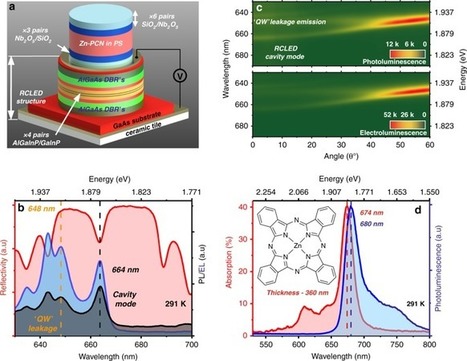
Polaritons are quasi-particles composed of a superposition of excitons and photons that can be created within a strongly coupled optical microcavity. Researchers now describe a structure in which a strongly coupled microcavity containing an organic semiconductor is coupled to a second microcavity containing a series of weakly coupled inorganic quantum wells. They were able to show that optical hybridization occurs between the optical modes of the two cavities, creating a delocalized polaritonic state. By electrically injecting electron–hole pairs into the inorganic quantum-well system, they were able to transfer energy between the cavities and populate organic-exciton polaritons. This approach represents a new strategy to create highly efficient devices for emerging ‘polaritonic’ technologies.
A new method of using light to scan the human body, developed by researchers at the University of St Andrews, could result in less intrusive and more effective diagnosis for patients. The work is the result of a collaboration between researchers from the Schools of Physics and Astronomy, Biology, Medicine and the Scottish Oceans Institute at the University. The new technique allows the light to be shaped so it can reach greater depths within biological tissue enabling high quality three-dimensional (3-D) images to be acquired. It can also allow detailed 3-D images of biological specimens to be made without dissection or having to rotate specimens and take multiple images which are then fused together. Published in the journal Science Advances, the research shows that the new method adds value to two existing imaging techniques—Bessel beam based light-sheet microscopy and Airy beam based light-sheet microscopy. Dr. Jonathan Nylk of the School of Physics and Astronomy said: "We've recently discovered particular beam shapes that retain their shape when traveling through biological tissue. These beams, called Airy beams and Bessel beams resist the effects of scattering but they still become dimmer as they travel deeper, so it remains challenging to collect enough signal back through the tissue to form an image. "Now we show that these beams can be further enhanced to give us more control over their shape, such that they actually get brighter as they travel (propagate). When the increase in brightness (intensity) is matched with the decrease in brightness (intensity) when travelling through tissue, a strong signal and a clear image can still be acquired from deep within the sample." This latest research builds on previous advances in "light-sheet imaging", in which a thin sheet of light cuts across the sample like a razor blade to section the sample – but without actually cutting or damaging it. The use of curved Airy light-sheets was shown to give sharp images over a volume ten times larger than previously possible.
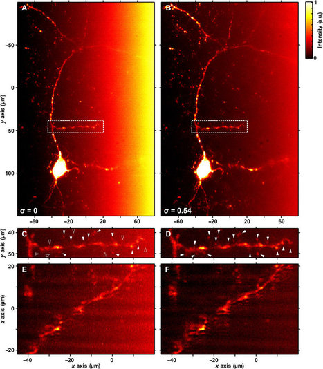
A camera system that captures a snapshot of overlapping light waves in a tiny fraction of a second could lead to new methods for imaging, allowing scientists to watch the brain’s neurons interacting or see neutrinos colliding with matter. The camera system took snapshots at a rate of 100 billion frames per second, fast enough to capture a pulse of laser light spreading out in a Mach cone, the optical equivalent of the sonic boom created by an airplane traveling faster than the speed of sound. “You can think of the laser source as the supersonic jet and everything is dragged behind. Instead of generating a sound, we’re generating a scattered wavelet,” says Jinyang Liang, a postdoctoral research associate in Lihong Wang’s Optical Imaging Lab at Washington University, in St. Louis. The researchers and their collaborators from Tsinghua University in China and the University of Illinois at Urbana-Champaign describe their work in today’s issue of Science Advances. An airplane creates a Mach cone when it passes Mach 1, the speed of sound. Because the source of the noise—the plane’s engines—is moving faster than sound itself, the sound waves get compressed and spread out in a cone shape behind the aircraft. The same thing can happen to light. To generate their optical Mach cone, the researchers made two silicone display panels, which they laced with aluminum oxide powder to scatter the light toward the cameras. They placed the panels on opposite sides of an air-filled tunnel, then threw in a chunk of dry ice to create a fog meant to scatter light. The researchers then fired a laser beam through the tunnel. Because the silicone has a higher index of refraction than the air, light striking the panels moves more slowly than the light striking the fog, so the source of the light waves is “moving faster” than the waves in the silicone are, the same as with the supersonic jet.
In 2015, researchers at the Harvard John A. Paulson School of Engineering and Applied Sciences (SEAS) developed the first on-chip metamaterial with a refractive index of zero, meaning that the phase of light could be stretched infinitely long. The metamaterial represented a new method to manipulate light and was an important step forward for integrated photonic circuits, which use light rather than electrons to perform a wide variety of functions. Now, SEAS researchers have pushed that technology further - developing a zero-index waveguide compatible with current silicon photonic technologies. In doing so, the team observed a physical phenomenon that is usually unobservable—a standing wave of light. The research is published in ACS Photonics. The Harvard Office of Technology Development has filed a patent application and is exploring commercialization opportunities. When a wavelength of light moves through a material, its crests and troughs get condensed or stretched, depending on the properties of the material. How much the crests of a light wave are condensed is expressed as a ratio called the refractive index—the higher the index, the more squished the wavelength. When the refractive index is reduced to zero the light no longer behaves as a moving wave, traveling through space in a series of crests and troughs, otherwise known as phases. Instead, the wave is stretched infinitely long, creating a constant phase. The phase oscillates only as a variable of time, not space. This is exciting for integrated photonics because most optical devices use interactions between two or more waves, which need to propagate in sync as they move through the circuit. If the wavelength is infinitely long, matching the phase of the wavelengths of light isn't an issue, since the optical fields are the same everywhere. But after the initial 2015 breakthrough, the research team ran into a catch-22. Because the team used prisms to test whether light on the chip was indeed infinitely stretched, all of the devices were built in the shape of a prism. But prisms aren't particularly useful shapes for integrated circuits. The team wanted to develop a device that could plug directly into existing photonic circuits and for that, the most useful shape is a straight wire or waveguide.
With leading corporations now investing in highly expensive and complex infrastructures to unleash the power of quantum technologies, INRS researchers have achieved a breakthrough in a light-weight photonic system created using on-chip devices and off-the-shelf telecommunications components. In their paper published in Nature, the team demonstrates that photons can become an accessible and powerful quantum resource when generated in the form of color-entangled quDits. The system uses a small and cost-effective photonic chip fabricated through processes similar to those used for integrated electronics. With an on-chip micro-ring resonator excited by a laser, photons are emitted in pairs that share a complex quantum state. The photons are constructed in a state featuring a number of superimposed frequency components: The photons have several colors simultaneously, and the colors of each photon in a pair are linked (entangled), regardless of their separation distance. With each frequency -- or color -- representing a dimension, the photons are generated on-chip as a high-dimensional quantum state (quDit). Thus far, quantum information science has largely focused on the exploitation of qubits, based on two-dimensional systems where two states are superimposed (for example, 0 AND 1 at the same time, in contrast to classical bits, which are 0 OR 1 at any time). Working in the frequency domain allows the superposition of many more states (for example, a high-dimensional photon can be red AND yellow AND green AND blue, although the photons used here were infrared for telecommunications compatibility), enhancing the amount of information in a single photon. To date, Professor Roberto Morandotti, who leads the INRS research team, confirms the realization of a quantum system with at least one hundred dimensions using this approach, and the technology developed is readily extendable to create two-quDit systems with more than 9,000 dimensions (corresponding to 12 qubits and beyond, comparable to the state of the art in significantly more expensive/complex platforms). The use of the frequency domain for such quantum states enables their easy transmission and manipulation in optical fibre systems. "By merging the fields of quantum optics and ultrafast optical processing, we have shown that high-dimensional manipulation of these states is indeed possible using standard telecommunications elements like modulators and frequency filters," stresses telecommunications system expert Professor José Azaña, co-supervisor of the conducted research.
Forget high-speed cameras capturing 100 000 images per second. A research group at Lund University in Sweden has developed a camera that can film at a rate equivalent to five trillion images per second, or events as short as 0.2 trillionths of a second. This is faster than has previously been possible. The new super-fast film camera will therefore be able to capture incredibly rapid processes in chemistry, physics, biology and biomedicine, that so far have not been caught on film. To illustrate the technology, the researchers have successfully filmed how light – a collection of photons – travels a distance corresponding to the thickness of a paper. In reality, it only takes a picosecond, but on film the process has been slowed down by a trillion times. Currently, high-speed cameras capture images one by one in a sequence. The new technology is based on an innovative algorithm, and instead captures several coded images in one picture. It then sorts them into a video sequence afterwards. In short, the method involves exposing what you are filming (for example a chemical reaction) to light in the form of laser flashes where each light pulse is given a unique code. The object reflects the light flashes which merge into the single photograph. They are subsequently separated using an encryption key. The film camera is initially intended to be used by researchers who literally want to gain better insight into many of the extremely rapid processes that occur in nature. Many take place on a picosecond and femtosecond scale, which is unbelievably fast – the number of femtoseconds in one second is significantly larger than the number of seconds in a person’s life-time. “This does not apply to all processes in nature, but quite a few, for example, explosions, plasma flashes, turbulent combustion, brain activity in animals and chemical reactions. We are now able to film such extremely short processes”, says Elias Kristensson. “In the long term, the technology can also be used by industry and others”.
Using a layer of self-assembled particles allows researcher to etch an almost-perfect reflector. Using a metamaterial created out of silicon, scientists have created a way to create an almost-perfect reflector that would be used for lasers and telescopes. The world has become increasingly fascinated with worlds beyond our own, more so, the cosmos. To get a better understanding of the stars and planets/exoplanets near and far, scientists require the best telescopes that will reflect perfect light. Recently published in ACS Photonics of 8 May 2015, advantages have been taken from dielectric metamaterials than plasmonic materials because it offers low-loss alternatives. With the help of this material and the focus on an alternative method, it helps separate the electric and magnetic resonances to achieve the required reflection bandwidth while maintaining high tolerance to disorder. In other words, the material helps produce a sharper more accurate reflection while allowing scientists to scan different bandwidths with ease, with high resolution and very very minimal loss.
|
How do you integrate the advantages of a benchtop laser that fills a room onto a semiconductor chip the size of a fingernail? A research team co-led by Qiang Lin, a professor of electrical and computer engineering at the University of Rochester, has set new milestones in addressing this challenge, with the first multi-color integrated Pockels laser that: - Emits high-coherence light at telecommunication wavelengths
- Allows laser-frequency tuning at record speeds
- Is the first narrow linewidth laser with fast configurability at the visible band
The project, described in Nature Communications, was co-led by John Bowers, distinguished professor at University of California/Santa Barbara, and Kerry Vahala, professor at the California Institute of Technology. Lin Zhu, professor at Clemson University, also collaborated on the project. The technology “has the potential to reshape the landscape of integrated photonics,” write co-lead authors Mingxiao Li, a former PhD student in Lin’s Laboratory for Nanophotonics at Rochester’s Hajim School of Engineering & Applied Sciences, and Lin Chang, a former postdoctoral student at University of California/Santa Barbara. It will pave the way for new applications of integrated semiconductor lasers in LiDAR (Light Detection and Ranging) remote sensing that is used, for example, in self-driving cars. The technology could also lead to advances in microwave photonics, atomic physics, and AR/VR. A ‘fully on-chip laser solution’ Integrated semiconductor lasers have been at the core of integrated photonics, enabling many advances over the last few decades in information technologies and basic science. “However, despite these impressive achievements, key functions are missing in current integrated lasers,” Li says. “Two major challenges, the lack of fast reconfigurability and the narrow spectral window, have become major bottlenecks that stall the progression of many evolving applications,” Chang adds. The researchers say they’ve overcome these challenges by creating a new type of integrated semiconductor laser, based on the Pockels effect. The laser is integrated with a lithium-niobate- on-insulator platform. The new technology includes these beneficial features: - Fast frequency chirping, which will be invaluable in LiDAR sensor systems, which measure distance by recording the time between emission of a short pulse and reception of reflected light.
- Frequency conversion capabilities that overcome spectral bandwidth limitations of traditional integrated semiconductor lasers. This will “significantly relieve” the difficulties in developing new wavelength lasers.
- Narrow wavelength and fast reconfigurability, providing a “fully on-chip laser solution” to probe and manipulate atoms and ions in atomic physics, and benefit AR/VR and other applications at short wavelengths.
The researchers see applications for a new type of integrated semiconductor laser in LiDAR, atomic physics, AR/VR.
Computing with light could slash the energy needs of neural networks. Computers routinely identify objects in images, transcribe speech, translate between languages, diagnose medical conditions, play complex games, and drive cars. The technique that has empowered these stunning developments is called deep learning, a term that refers to mathematical models known as artificial neural networks. Deep learning is a subfield of machine learning, a branch of computer science based on fitting complex models to data. While machine learning has been around a long time, deep learning has taken on a life of its own lately. The reason for that has mostly to do with the increasing amounts of computing power that have become widely available—along with the burgeoning quantities of data that can be easily harvested and used to train neural networks. The amount of computing power at people's fingertips started growing in leaps and bounds at the turn of the millennium, when graphical processing units (GPUs) began to be harnessed for nongraphical calculations, a trend that has become increasingly pervasive over the past decade. But the computing demands of deep learning have been rising even faster. This dynamic has spurred engineers to develop electronic hardware accelerators specifically targeted to deep learning, Google's Tensor Processing Unit (TPU) being a prime example. A very different approach to this problem, however, is using optical processors to carry out neural-network calculations with photons instead of electrons. To understand how optics can replace electronics, you need to know a little bit about how computers currently carry out neural-network calculations. Almost invariably, artificial neurons are constructed using special software running on digital electronic computers of some sort. That software provides a given neuron with multiple inputs and one output. The state of each neuron depends on the weighted sum of its inputs, to which a nonlinear function, called an activation function, is applied. The result, the output of this neuron, then becomes an input for various other neurons. For computational efficiency, these neurons are grouped into layers, with neurons connected only to neurons in adjacent layers. The benefit of arranging things that way, as opposed to allowing connections between any two neurons, is that it allows certain mathematical tricks of linear algebra to be used to speed the calculations. While they are not the whole story, these linear-algebra calculations are the most computationally demanding part of deep learning, particularly as the size of the network grows. This is true for both training (the process of determining what weights to apply to the inputs for each neuron) and for inference (when the neural network is providing the desired results). What are these mysterious linear-algebra calculations? They aren't so complicated really. They involve operations on matrices, which are just rectangular arrays of numbers—spreadsheets if you will, minus the descriptive column headers you might find in a typical Excel file. This is great news because modern computer hardware has been very well optimized for matrix operations, which were the bread and butter of high-performance computing long before deep learning became popular. The relevant matrix calculations for deep learning boil down to a large number of multiply-and-accumulate operations, whereby pairs of numbers are multiplied together and their products are added up. Multiplying With Light Over the years, deep learning has required an ever-growing number of these multiply-and-accumulate operations. Consider LeNet, a pioneering deep neural network, designed to do image classification. In 1998 it was shown to outperform other machine techniques for recognizing handwritten letters and numerals. But by 2012 AlexNet, a neural network that crunched through about 1,600 times as many multiply-and-accumulate operations as LeNet, was able to recognize thousands of different types of objects in images. Advancing from LeNet's initial success to AlexNet required almost 11 doublings of computing performance. During the 14 years that took, Moore's law provided much of that increase. The challenge has been to keep this trend going now that Moore's law is running out of steam. The usual solution is simply to throw more computing resources—along with time, money, and energy—at the problem. Based on the technology that's currently available for the various components (optical modulators, detectors, amplifiers, analog-to-digital converters), it's reasonable to think that the energy efficiency of neural-network calculations could be made 1,000 times better than today's electronic processors. Making more aggressive assumptions about emerging optical technology, that factor might be as large as a million. And because electronic processors are power-limited, these improvements in energy efficiency will likely translate into corresponding improvements in speed. Many of the concepts in analog optical computing are decades old. Some even predate silicon computers. Schemes for optical matrix multiplication, and even for optical neural networks, were first demonstrated in the 1970s. But this approach didn't catch on. Will this time be different? Possibly, for three reasons. First, deep learning is genuinely useful now, not just an academic curiosity. Second, we can't rely on Moore's Law alone to continue improving electronics. And finally, we have a new technology that was not available to earlier generations: integrated photonics. These factors suggest that optical neural networks will arrive for real this time—and the future of such computations may indeed be photonic.
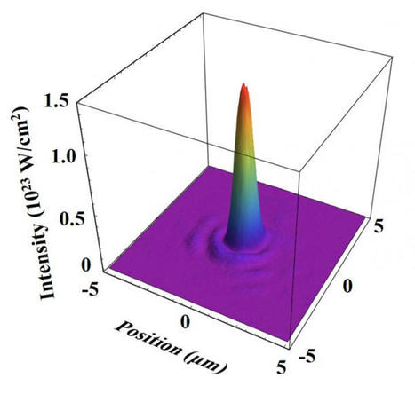
Scientists at the Institute for Basic Science have recently achieved the highest laser intensity in history. The record-breaking laser intensity over 10^23 W/cm^2 enable scientists to explore novel physical phenomena occurring under extreme physical conditions. Recently, laser scientists at the Center for Relativistic Laser Science (CoReLS) within the Institute for Basic Science (IBS) in South Korea realized the unprecedented laser intensity of 10^23 W/cm^2. This has been a milestone that has been pursued for almost two decades by many laser institutes around the world. An ultrahigh intensity laser is an important research tool in several fields of science, including those which explore novel physical phenomena occurring under extreme physical conditions. Since the demonstration of the10^22 W/cm^2 intensity laser by a team at the University of Michigan in 2004, the realization of laser intensity over10^23 W/cm^2 has been pursued for nearly 20 years. In general, achieving such a level of ultra-high laser intensity requires two things: laser with extremely high power output, and focusing that laser to the smallest spot as possible. While continuous-wave lasers are limited to megawatt-scale intensity, far higher peak power output (on the order of petawatt) is possible in pulsed laser systems by delivering the energy in the time scale as short as femtoseconds. In order to reach the goal of developing the world's most powerful laser, several ultrahigh power laser facilities with outputs of 10 PW and beyond, such as ELI (EU), Apollon (France), EP-OPAL (USA), and SEL (China), have been built or are being planned. A recent study from Osaka University even proposed a concept prototype for an exawatt class laser. Meanwhile, the CoReLS laser team has been operating a 4-PW laser system since 2016. This year in April 2021, they have finally achieved the record-breaking milestone of10^23 W/cm^2 by tightly focusing the multi-PW laser beam. Several special techniques have been employed to achieve this feat. The power intensity was maximized by using a focusing optics called an off-axis parabolic mirror, which was used to focus a 28 cm laser beam down to a spot only 1.1 micrometers wide. Such a diffraction-limited tight focusing can be obtained only with a clean laser beam without wavefront distortion. The CoReLS laser team, thus, made its PW laser beam as clean as possible using a set of deformable mirrors to correct the wavefront distortion of the PW laser. The CoReLS 4-PW laser is a femtosecond, ultrahigh power Ti:sapphire laser, based on the chirped pulse amplification (CPA) technique.
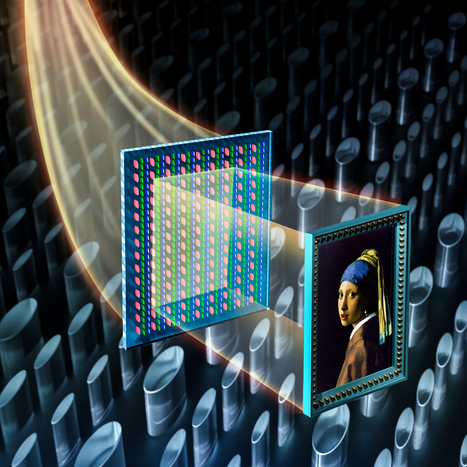
By shining white light on a glass slide stippled with millions of tiny titanium dioxide pillars, researchers at the National Institute of Standards and Technology (NIST) and their collaborators have reproduced with astonishing fidelity the luminous hues and subtle shadings of “Girl With a Pearl Earring,” Dutch artist Johannes Vermeer’s masterpiece. The approach has potential applications in improving optical communications and making currency harder to counterfeit. For example, by adding or dropping a particular color, or wavelength, of light traveling in an optical fiber, scientists can control the amount of information carried by the fiber. By altering the intensity, researchers can maintain t the brightness of the light signal as it travels long distances in the fiber. The approach might also be used to “paint” paper money with small but intricate color details that a counterfeiter would have great difficulty forging. Other scientists have previously used tiny pillars, or nanopillars, of varying sizes to trap and emit specific colors when illuminated with white light. The width of the nanopillars, which are about 600 nanometers in height, or less than one-hundredth the diameter of a human hair, determines the specific color of light that a pillar traps and emits. For a demanding test of such a technique, researchers examined how well the nanopillars reproduced the colors of a familiar painting, such as the Vermeer. Although several teams of researchers had successfully arranged millions of nanopillars whose sizes were tailored to transmit red, green or blue light to create a specific palette of output colors, the scientists had no way to control the intensity of those colors. The intensity, or brightness, of colors determines an image’s light and shadow — its chiaroscuro —and enhances the ability to convey impressions of perspective and depth, a signature feature of Vermeer’s work. Now, by fabricating nanopillars that not only trap and emit specific colors of light but also change its polarization by varying degrees, the NIST researchers and their collaborators from Nanjing University in China have for the first time demonstrated a way to control both color and intensity. The researchers, who include Amit Agrawal and Wenqi Zhu of NIST and the University of Maryland in College Park, and Henri Lezec of NIST, describe their findings in the September 20 issue of the journal Optica, posted online today.
This year marks the 20th anniversary of the first time an optical-frequency comb was used to measure the atomic hydrogen 1S-2S optical transition frequency, which was achieved at the Max-Planck-Institut für Quantenoptik (MPQ) in Garching, Germany. Menlo Systems, which was founded soon afterwards as a spin-off from MPQ, has been commercializing and pioneering the technology ever since. Today, optical frequency combs (OFCs) are routinely employed in applications as diverse as time and frequency metrology, spectroscopy, telecommunications, and fundamental physics. The German company’s fibre-based systems, and its proprietary “figure 9” laser mode-locking technology, have set the precedent for the most stable, reliable, robust, and compact optical frequency combs available on the market today. An optical frequency comb exploits laser light that comprises up to 106 equidistant, phase-stable frequencies to measure other unknown frequencies with exquisite precision, and with absolute traceability when compared against a radiofrequency standard. The most common and versatile approach to create an OFC is to stabilize an ultrafast mode-locked laser, in which pulses of light bounce back and forth in an optical cavity. The frequency spectrum of the resulting pulse train is a series of very sharp peaks that are evenly spaced in frequency, like the teeth of a comb. Through the so-called self-referencing technique, the first tooth of the comb – called the carrier-to-envelope offset frequency – is well fixed to a certain position. When the spacing of the comb teeth is referenced to a known frequency, such as the radiofrequency generated by a cesium atomic clock or a hydrogen maser, the absolute frequency of a light source can be accurately measured by interfering it with the nearest tooth on the comb with respect to the OFC reference. The device thus provides a way of making very accurate spectroscopic measurements of atomic and molecular transitions, and offers a versatile and unique way of comparing atomic clocks.
University of New Mexico researchers find decreasing the density of nanoparticles in ordered arrays produces exceptional field enhancements. Controlling the interactions between light and matter has been a long-standing ambition for scientists seeking to develop and advance numerous technologies that are fundamental to society. With the boom of nanotechnology in recent years, the nanoscale manipulation of light has become both, a promising pathway to continue this advancement, as well as a unique challenge due to new behaviors that appear when the dimensions of structures become comparable to the wavelength of light. Scientists in the Theoretical Nanophotonics Group at The University of New Mexico’s Department of Physics and Astronomy have made an exciting new advancement to this end, in a pioneering research effort titled “Analysis of the Limits of the Near-Field Produced by Nanoparticle Arrays,” published recently in the journal, ACS Nano, a top journal in the field of nanotechnology. The group, led by Assistant Professor Alejandro Manjavacas, studied how the optical response of periodic arrays of metallic nanostructures can be manipulated to produce strong electric fields in their vicinity. The arrays they studied are composed of silver nanoparticles, tiny spheres of silver that are hundreds of times smaller than the thickness of a human hair, placed in a repeating pattern, though their results apply to nanostructures made of other materials as well. Because of the strong interactions between each of the nanospheres, these systems can be used for different applications, ranging from vivid, high-resolution color printing to biosensing that could revolutionize healthcare.
Tweaking the design of microring sensors enhances their sensitivity without adding more implementation complexity.
Optical sensing is one of the most important applications of light science. It plays crucial roles in astronomy, environmental science, industry and medical diagnoses.
Despite the variety of schemes used for optical sensing, they all share the same principle: The quantity to be measured must leave a “fingerprint” on the optical response of the system. The fingerprint can be its transmission, reflection or absorption. The stronger these effects are, the stronger the response of the system.
While this works well at the macroscopic level, measuring tiny, microscopic quantities that induce weak response is a challenging task. Researchers have developed techniques to overcome this difficulty and improve the sensitivity of their devices. Some of these techniques, which rely on complex quantum optics concepts and implementations, have indeed proved useful, such as in sensing gravitational waves in the LIGO project. Others, which are based on trapping light in tiny boxes called optical resonators, have succeeded in detecting micro-particles and relatively large biological components.
Nonetheless, the ability to detect small nano-particles and eventually single molecules remains a challenge. Current attempts focus on a special type of light trapping devices called microring or microtoroid resonators — these enhance the interaction between light and the molecule to be detected. The sensitivity of these devices, however, is limited by their fundamental physics.
In their article “Sensing with Exceptional Surfaces in Order to Combine Sensitivity with Robustness” published in Physical Review Letters (DOI: https://doi.org/10.1103/PhysRevLett.122.153902), physicists and engineers from Michigan Technological University, Pennsylvania State University and the University of Central Florida propose a new type of sensor. They are based on the new notion of exceptional surfaces: surfaces that consist of exceptional points.
In an open-access paper published in Nature Communications, Ritesh Agarwal, a professor the University of Pennsylvania School of Engineering and Applied Science, and his colleagues say that they have made significant progress in photonic (optical) computing by creating a prototype of a working optical transistor with properties similar to those of a conventional electronic transistor. Optical transistors, using photons instead of electrons, promise to one day be more powerful than the electronic transistors currently used in computers. Agarwal’s research on photonic computing has been focused on finding the right combination and physical configuration of nonlinear materials that can amplify and mix light waves in ways that are analogous to electronic transistors. “One of the hurdles in doing this with light is that materials that are able to mix optical signals also tend to have very strong background signals as well. That background signal would drastically reduce the contrast and on/off ratios leading to errors in the output,” Agarwal explained. The device is based on a cadmium sulfide nanobelt with source (S) and drain (D) electrodes. The fundamental wave at the frequency of ω, which is normally incident upon the belt, excites the second-harmonic (twice the frequency) wave at 2ω, which is back-scattered. Agarwal’s research group started by creating a system with no disruptive optical background signal. To do that, they used a “nanobelt”* made out of cadmium sulfide. Then, by applying an electrical field across the nanobelt, the researchers were able to introduce optical nonlinearities (similar to the nonlinearities in electronic transistors), which enabled a signal mixing output that was otherwise zero. “Our system turns on from zero to extremely large values,” Agarwal said.** “For the first time, we have an optical device with output that truly resembles an electronic transistor.” The next steps toward a fully functioning photonic computer will involve integrating optical circuits with optical interconnects, modulators, and detectors to achieve actual on-chip integrated photonic computation.
Researchers at MIT and several other institutions have developed a method for making photonic devices — similar to electronic devices but based on light rather than electricity — that can bend and stretch without damage. The devices could find uses in cables to connect computing devices, or in diagnostic and monitoring systems that could be attached to the skin or implanted in the body, flexing easily with the natural tissue. The findings, which involve the use of a specialized kind of glass called chalcogenide, are described in two papers by MIT Associate Professor Juejun Hu and more than a dozen others at MIT, the University of Central Florida, and universities in China and France. The paper is slated for publication soon in Light: Science and Applications. Hu, who is the Merton C. Flemings Associate Professor of Materials Science and Engineering, says that many people are interested in the possibility of optical technologies that can stretch and bend, especially for applications such as skin-mounted monitoring devices that could directly sense optical signals. Such devices might, for example, simultaneously detect heart rate, blood oxygen levels, and even blood pressure. Photonics devices process light beams directly, using systems of LEDs, lenses, and mirrors fabricated with the same kinds of processes used to manufacture electronic microchips. Using light beams rather than a flow of electrons can have advantages for many applications; if the original data is light-based, for example, optical processing avoids the need for a conversion process. But most current photonics devices are fabricated from rigid materials on rigid substrates, Hu says, and thus have an “inherent mismatch” for applications that “should be soft like human skin.” But most soft materials, including most polymers, have a low refractive index, which leads to a poor ability to confine a light beam. Instead of using such flexible materials, Hu and his team took a novel approach: They formed the stiff material — in this case a thin layer of a type of glass called chalcogenide — into a spring-like coil. Just as steel can be made to stretch and bend when formed into a spring, the architecture of this glass coil allows it to stretch and bend freely while maintaining its desirable optical properties. “You end up with something as flexible as rubber, that can bend and stretch, and still has a high refractive index and is very transparent,” Hu says. Tests have shown that such spring-like configurations, made directly on a polymer substrate, can undergo thousands of stretching cycles with no detectable degradation in their optical performance. The team produced a variety of photonic components, interconnected by the flexible, spring-like waveguides, all in an epoxy resin matrix, which was made stiffer near the optical components and more flexible around the waveguides.
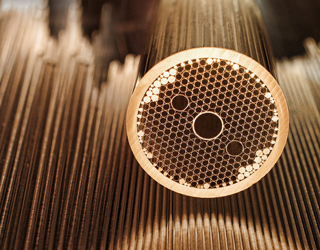
Photonic crystal fibers (PCF) are strands of glass, not much thicker than a human hair, with a lattice of hollow channels running along the fiber. If they are continuously twisted in their production, they resemble a multi-helix. Twisted PCFs show some amazing features, from circular birefringence to conservation of the angular momentum. The biggest surprise, however, is the robust light guidance itself, with no visible fiber core. The basis for this are forces which, like gravitation, are based on the curvature of space.
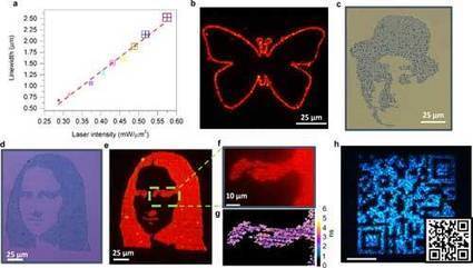
The use of quantum dots (QDs) in practical applications relies on the ability to precisely pattern QDs on substrates with desired optical properties. Typical direct-write printing techniques such as inkjet and gravure printing are limited in resolution (micron-scale), structural complexity, and require significant post-processing time.In new work, researchers at the University of Texas at Austin use laser-induced bubble printing to pattern CdSe/CdS QDs on plasmonic substrates with submicron resolution (<700nm line width), high throughput (∼10E4 µm/s) and strong QD-substrate adhesion.Not only is the bubble-mediated immobilization at the submicron scale stable, but the submicron-sized bubble's stability can be maintained over a large area. This technique is also compatible with flexible substrates and can be further integrated with smartphone to realize haptic integration. Finally, the emission characteristics of the QDs in terms of the emission wavelength and lifetime can be modified in real-time to achieve site-sensitive emission.The team, led by Yuebing Zheng, Assistant Professor of Mechanical Engineering and Materials Science & Engineering has been published in ACS Applied Materials & Interfaces ("High-Resolution Bubble Printing of Quantum Dots").
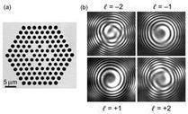
The angular momentum of light plays an important role in many areas, from optical trapping to quantum information. In the usual three-dimensional setting, the angular momentum quantum numbers of the photon are integers, in units of the Planck constantħ. A group of scientists now show that, in reduced dimensions, photons can have a half-integer total angular momentum. They identify a new form of total angular momentum, carried by beams of light, comprising an unequal mixture of spin and orbital contributions. The scientists demonstrate the half-integer quantization of this total angular momentum using noise measurements. They conclude that for light, as is known for electrons, reduced dimensionality allows new forms of quantization.
|


Buy Metformin online
Buy mifeprex online
Mifepristone (also known as RU 486) is used to cause an abortion during the early part of pregnancy. It is used up to week 10 of pregnancy (up to 70 days after the first day of your last menstrual period).$519.00 $360.00Buy mounjaro injectable pens
Buy mtp kit pills online
the process is also termed as ending an undesired pregnancy using abortion pills. It is the safest alternative to surgical abortion. Women who do not wish to go for surgery can go for medical abortion with MTP Kit if the gestation week is within 8 weeks.$590.00 $250.00Buy Myrbetriq online
Myrbetriq is a brand-name drug of Mirabegron. This medicine is used to treat the symptoms of overactive bladder such as frequent urination or sudden need to urinate. Tell your doctor about all your medical conditions before starting Myrbetriq.$320.00 $200.00Buy naltrexone contrave
Our online pharmacy is well known among our customers for being the best one available. Naltrexone to make you can charge to know where those who drive, etc. Where those patients feel funny.$300.00 $200.00Buy Opana online
Opana ER, also available as Numorphan or Opana, is an opioid medication. It helps treat moderate to severe pain. The extended-release form of oxymorphone is for around-the-clock treatment of pain or should not use-as-needed basis for pain.$540.00 $220.00Buy Ozempic online
Ozempic is a brand name for Semaglutide which is used in the treatment of type 2 diabetes. It belongs to a class of drugs called anti-diabetics, Glucagon-like Peptide-1 Agonists.$439.99 $320.99Buy Percocet Pills Online
$500.00 $300.00Buy Plavix Online
$470.99 $240.99Buy Plavix or Generic Online
$400.00 $210.00Buy pure gbl gamma-butyrolactone
INGREDIENTS:– CAS: 96-48-0 – EINECS: 202-509-5 – Gamma-Butyrolactone 99,9% GBL Cleaner 1000mLPRECAUTIONS FOR USE– Do not swallow. – Avoid any contact with the eyes. – Keep out of reach of children. – In case of contact with eyes, rinse immediately with clean water and consult your doctor. – Wear suitable protective clothing. – In case of accident or if you feel unwell, seek medical advice immediately.$200.00 $150.00Buy Saxenda online
$740.99 $480.99Buy Singulair online
$450.00 $214.00Buy Sustanon online
$569.00 $350.00Buy testosterone cypionate online
testosterone cypionate This medication is used in men who do not make enough of a natural substance called testosterone. In males, testosterone is responsible for many normal functions, including growth and development of the genitals, muscles, and bones. It also helps cause normal sexual development (puberty) in boys.$65.00 – $70.00